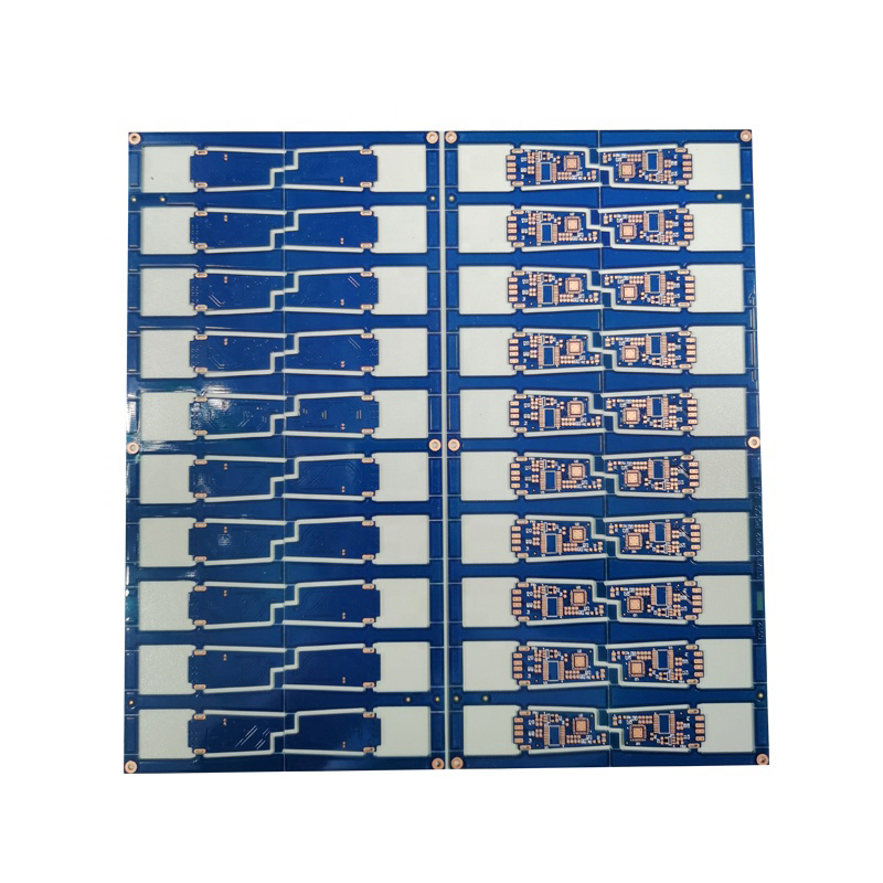
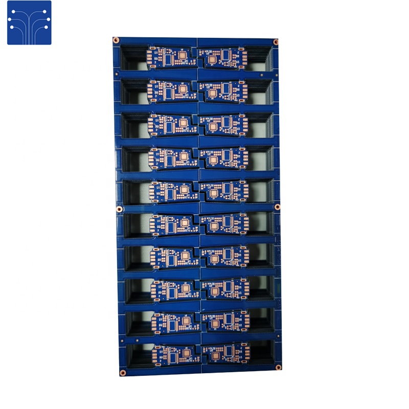
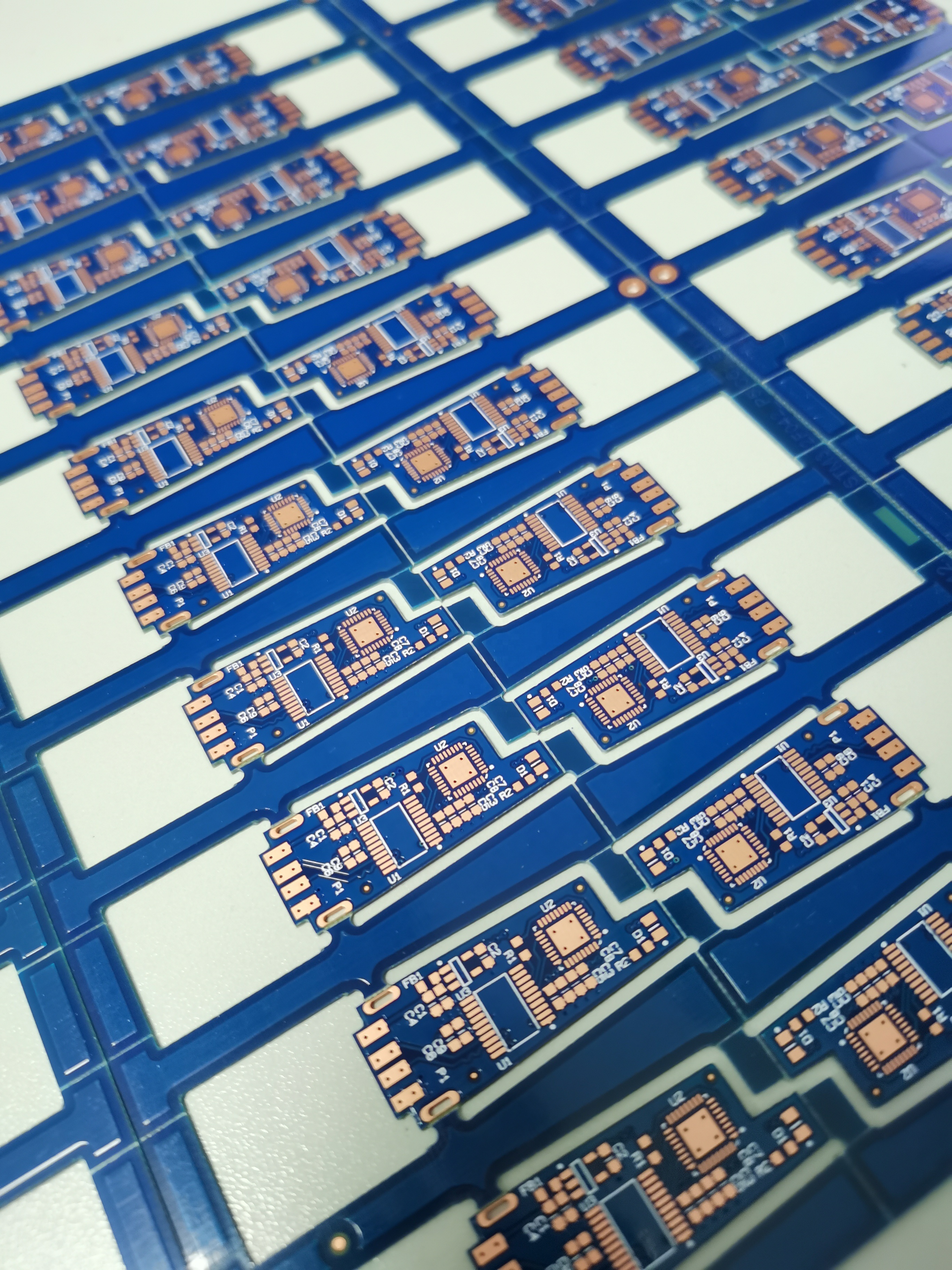
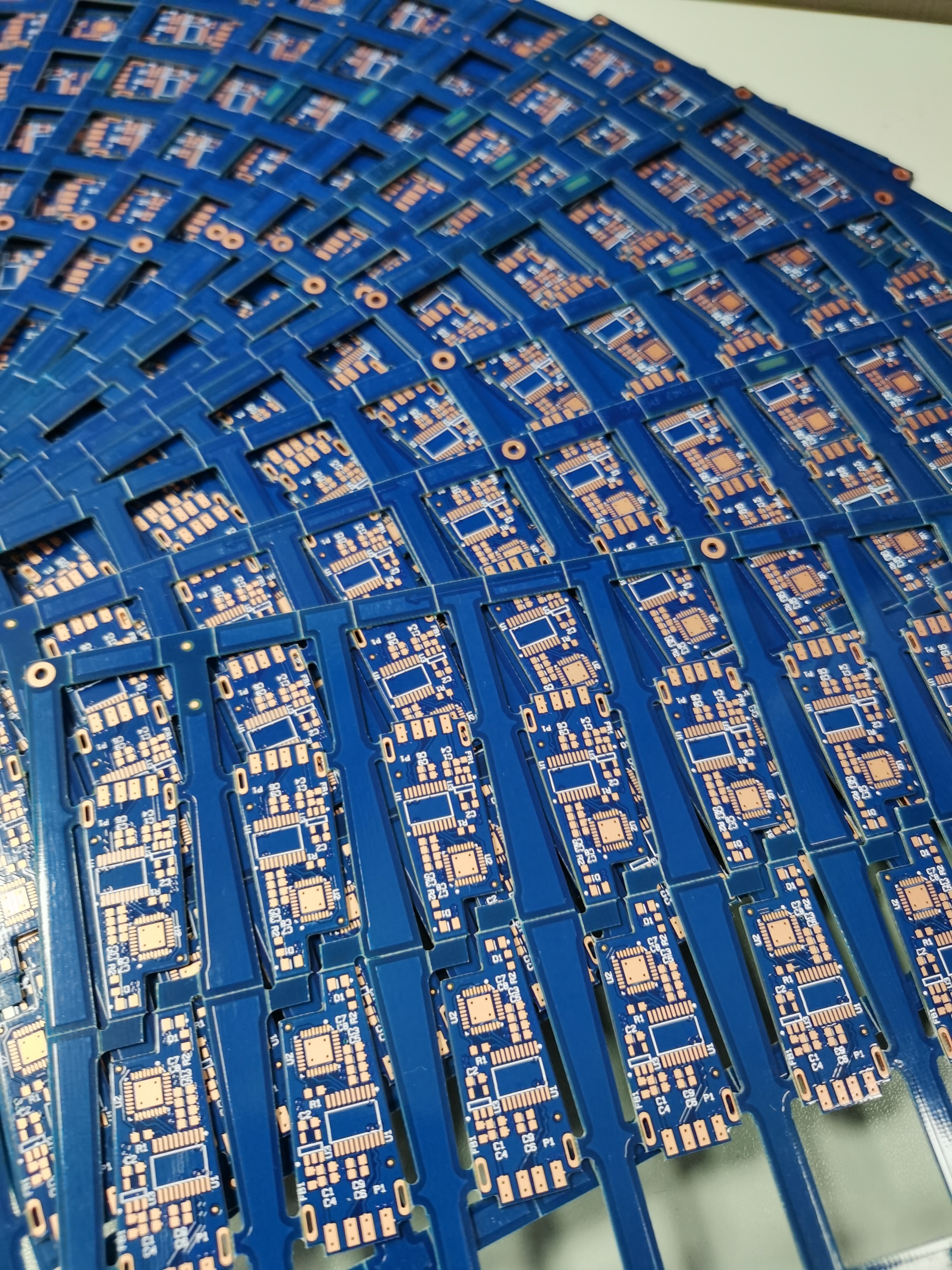
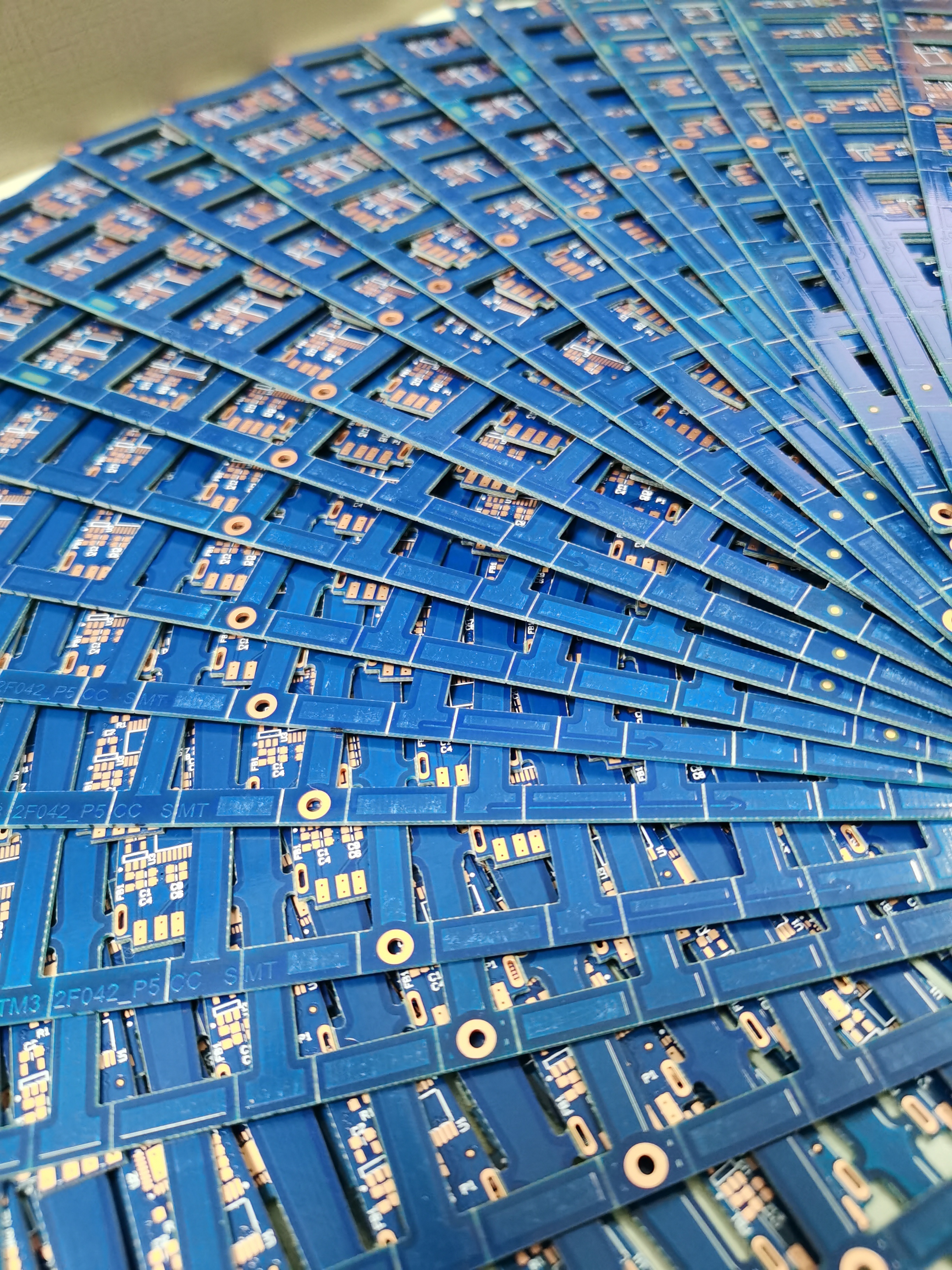
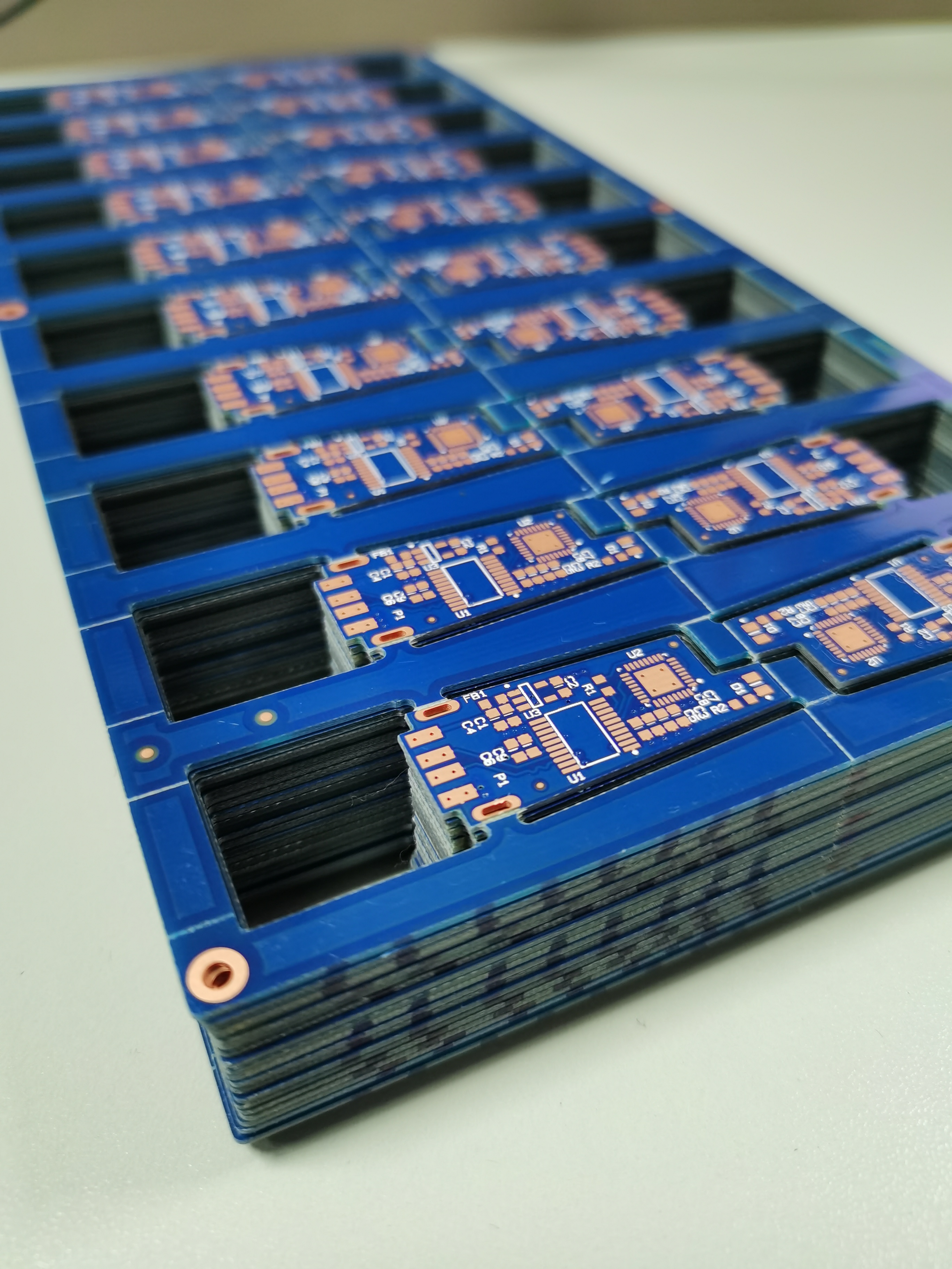
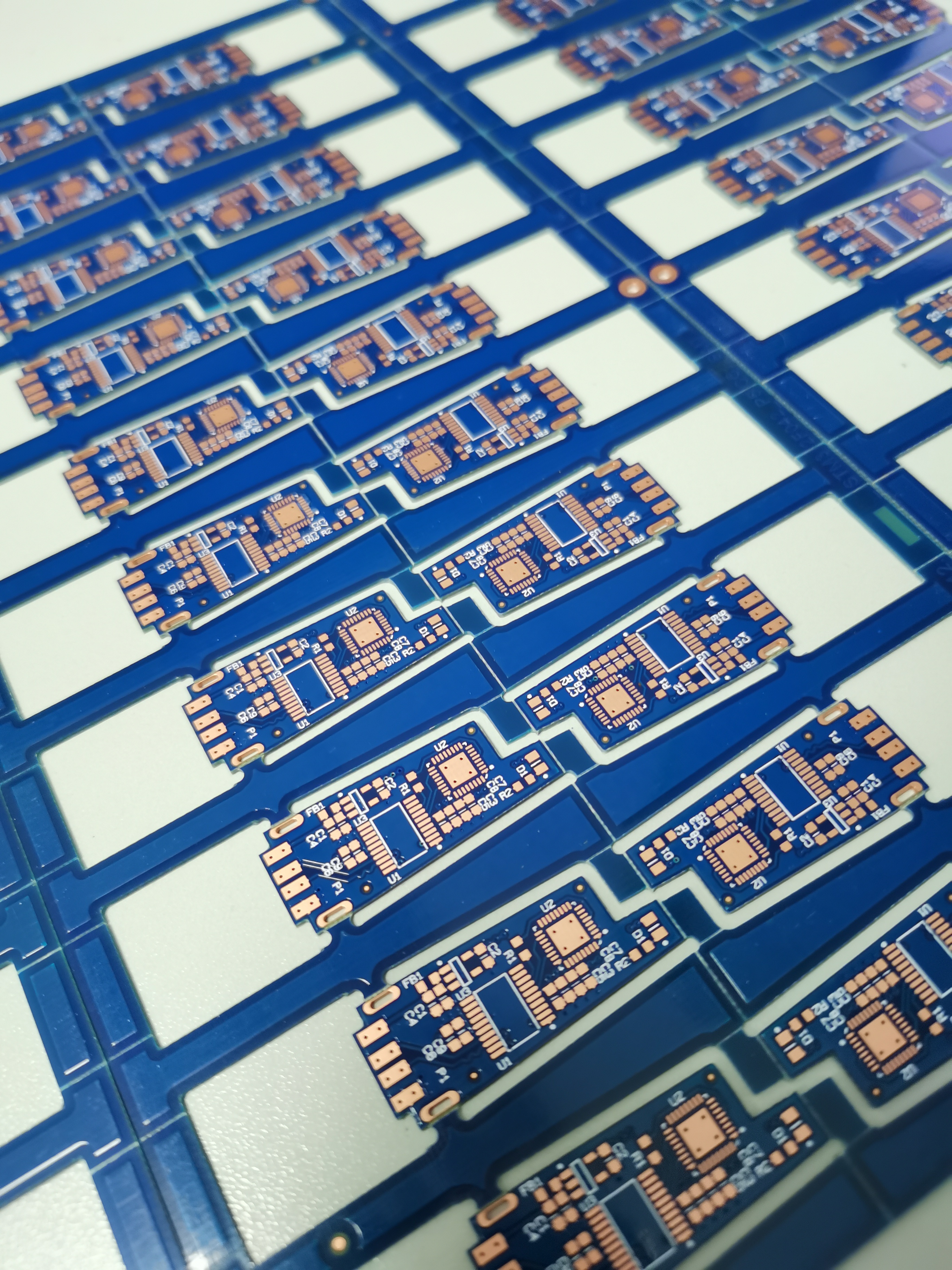
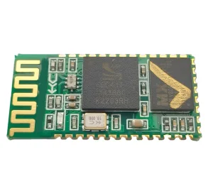
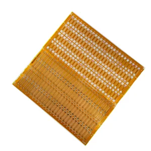
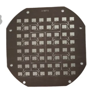
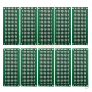
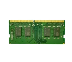
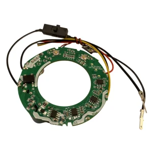
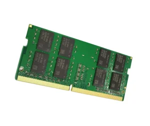
TOP PCB Double Layer Board PCB Printing Making Machine China Manufacture Projector double side PCB design

Product Description

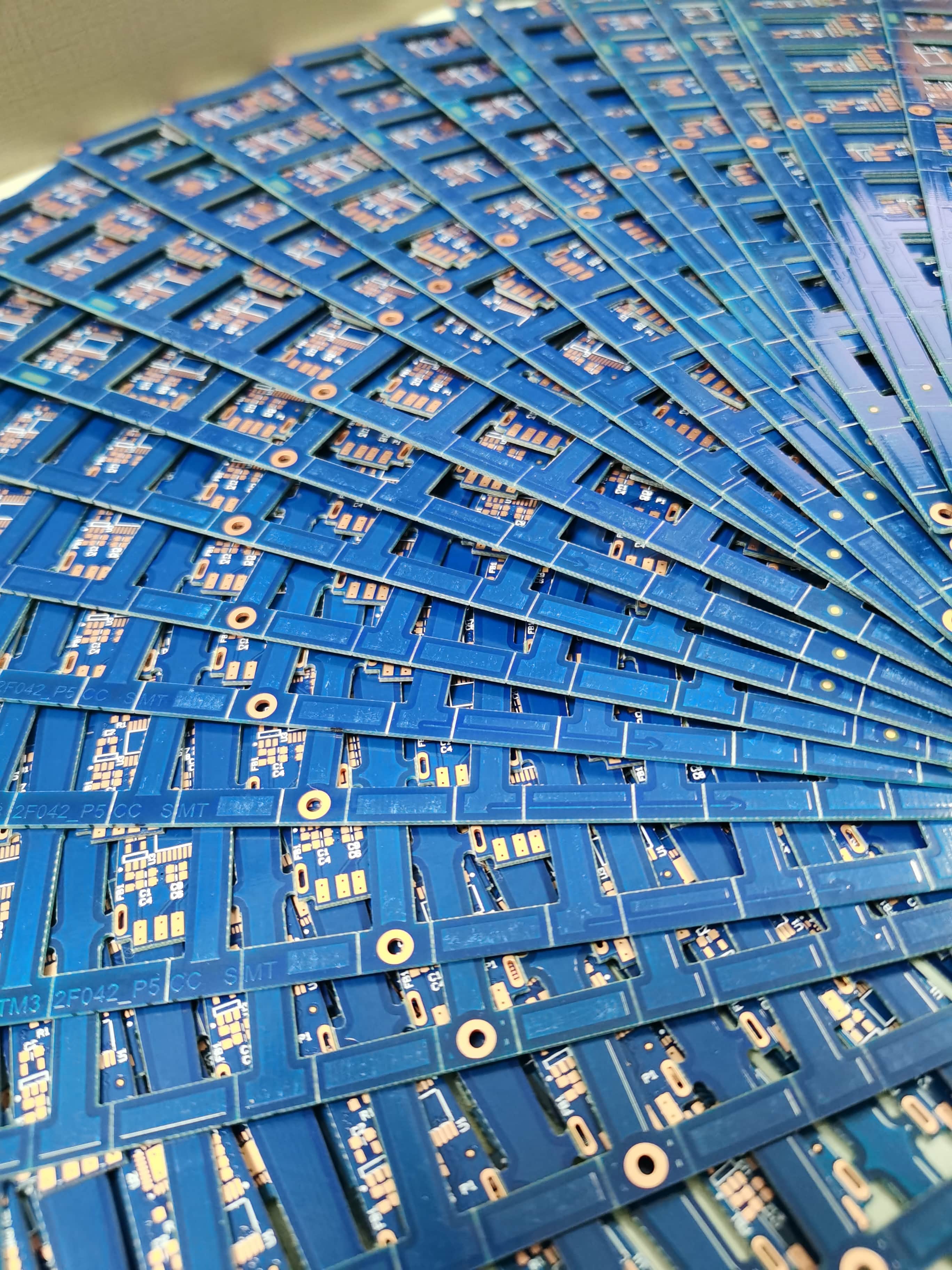
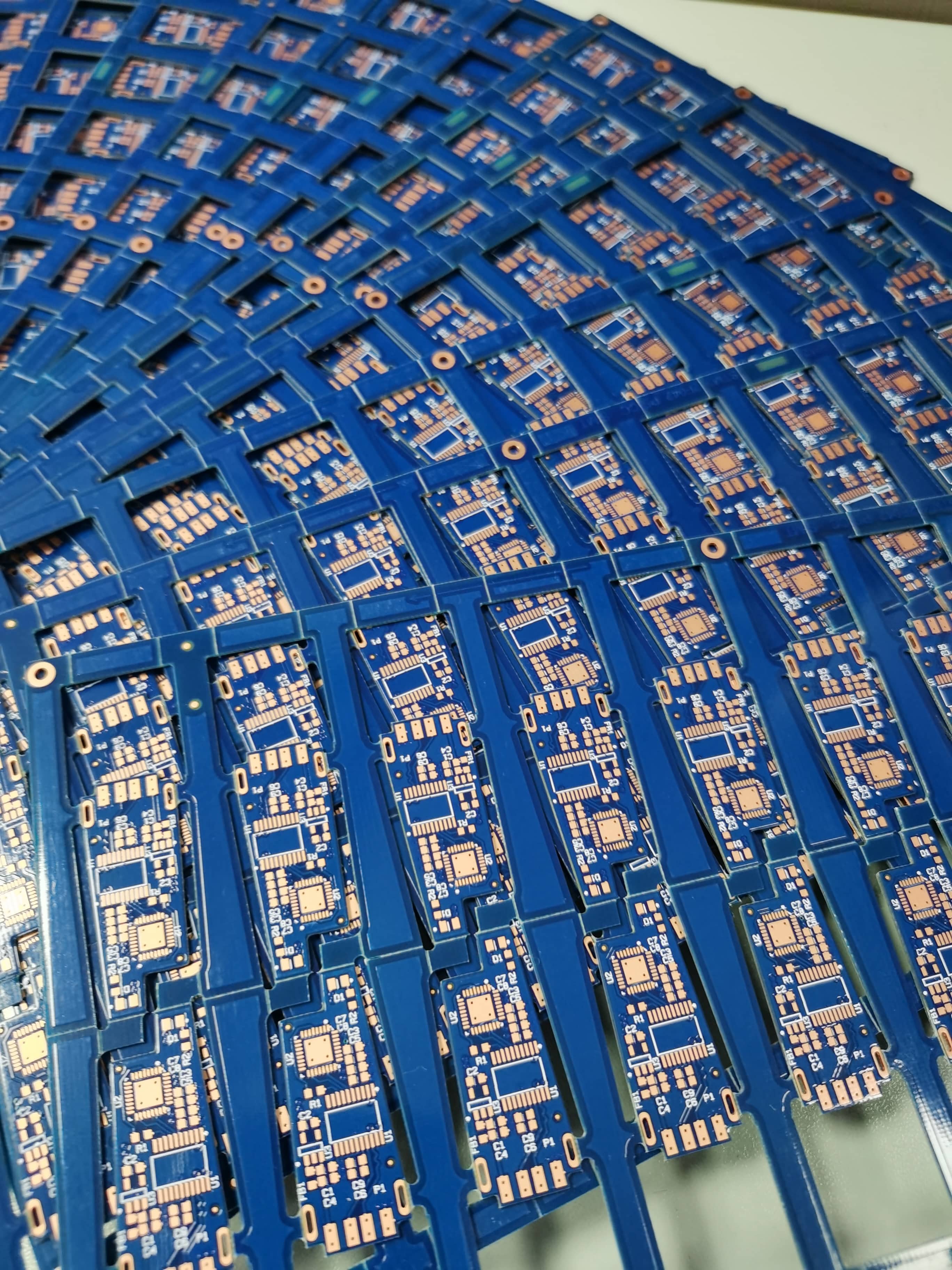
PCB Board Manufacturing
TOP PCB Double Layer Board PCB Printing Making Machine China Manufacture Projector Double Side PCB Design
Product Description
Our Advantages:
Free program and functional test and package.
High quality standards: IPC-A-610E, E-test, X-ray, AOI test, 100% functional test.
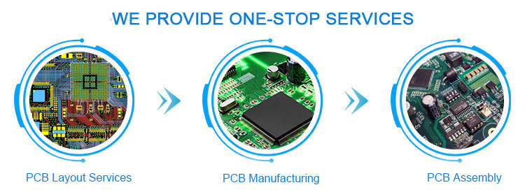
Professional one-stop service: PCB/FPC/Aluminium Making, SMT, DIP, Component Sourcing.
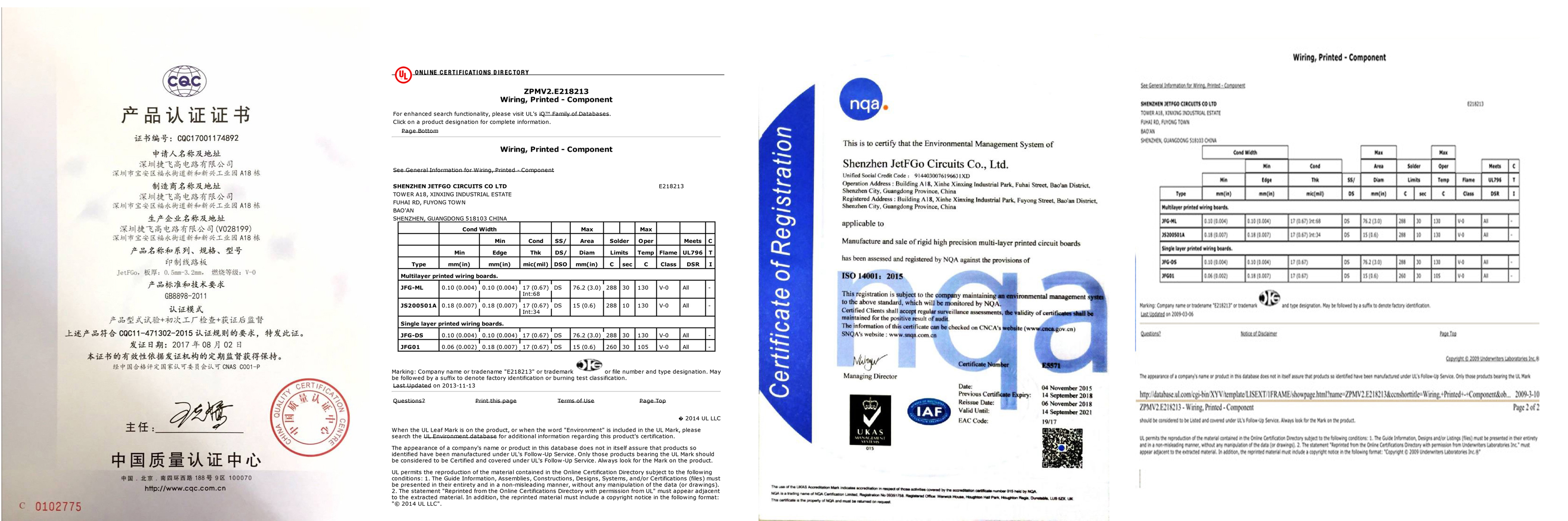
Full Certifications: UL, CE, SGS, FCC, RoHS, ISO9001, ISO13485, TS16949.
PCB & PCBA Capacity:
Items Capacity
Material FR4, (High Tg, General Tg, Middle Tg), Halogen Free FR4, Ceramic, Teflon, PI, BT, PPO, PPE etc.
Board thickness Mass production: 10mm; Samples: 17.5mm
Surface finish HASL, Immersion Gold/Tin, OSP, ENIG + OSP, Immersion Silver, ENEPIG, Gold Finger
PCB Max panel size 1150mm × 560mm
Layer Count Mass production: 2~58 layers; Pilot run: 64 layers; Flexible PCB: 1-12 Layers
Min hole size Mechanical drill: 8mil(0.2mm); Laser drill: 3mil(0.075mm)
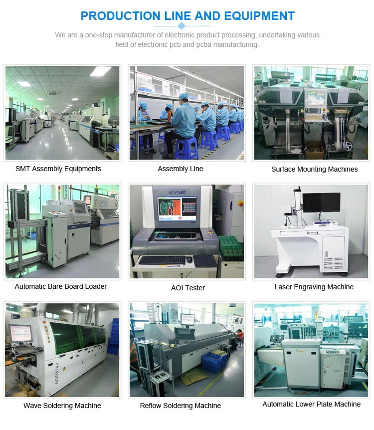
PCBA QC X-ray, AOI Test, Functional Test
Special Process Buried Hole, Blind Hole, Embedded Resistance/Capacity, Hybrid, Back drilling.
SMT/DIP Capacity SMT: 700M Points/Day; DIP: 0.5M Points/Day
Product Display
About Us

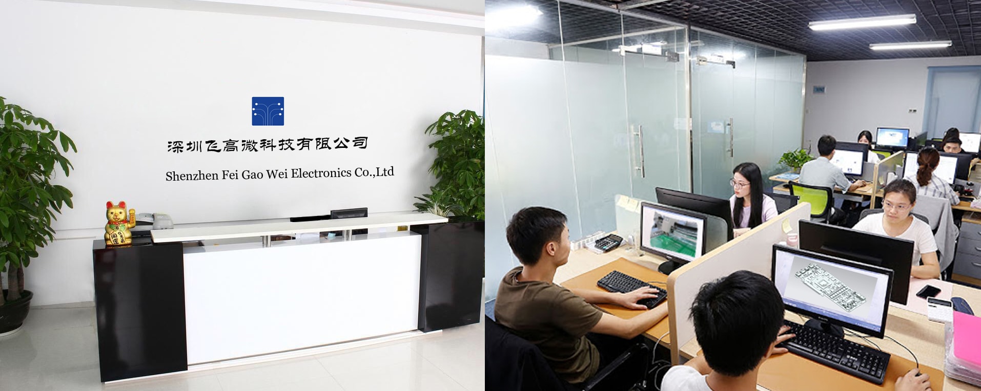
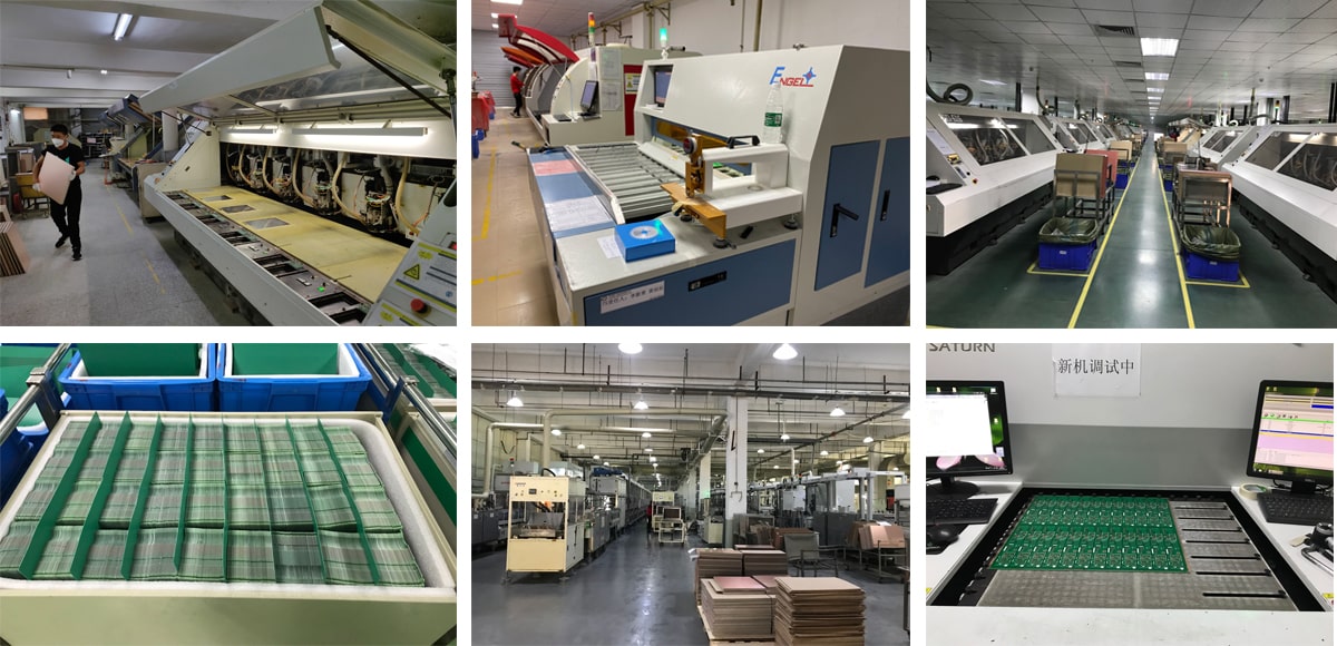
Comprehensive Electronics Services: We provide Schematic Design & Board Layout, PCB & FPC Manufacturing, Metal Injection Molding, and Global Supply Chain Management. Our services deliver finished goods directly to you or via drop shipping. We maintain the flexibility to match your specific technical needs.

One-Stop PCBA Solutions: Specialized in 0201/BGA/CCGA surface-mount (SMT), thru-hole (THT), mixed technology, conformal coating, potting, and encapsulations. Testing includes AOI, X-Ray, and full functional testing. Applications cover telecommunications, automotive, 5G, IOT, AI smart control, industrial, and medical fields.
Certificates & Feedback
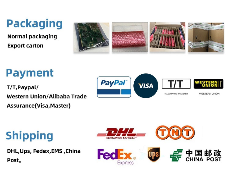
Packing & Shipping
FAQ
1. What files do you use in PCBA fabrication?
We use Gerber or Eagle files, BOM listing, PNP, and Components Position data.
2. Is it possible to offer a sample?
Yes, we can provide custom samples for your testing before moving to mass production.
3. How quickly can I get a quotation?
PCB quotations are typically provided within 6 hours, and PCBA quotations within 24 hours after receiving Gerber and BOM files.
4. What is the typical production timeline?
PCB production and component purchasing take 7-10 days, followed by approximately 10 days for assembly and testing.
5. Are my designs secure with you?
Yes, your files are held in complete safety. We respect copyright and your files are never shared with third parties.
6. Do you have a Minimum Order Quantity (MOQ)?
We have no MOQ. We have the capability to produce prototype circuit boards in any amount for small quantity orders.

Related Products