Explore our elite engineering products, from high-sensitivity PCBs to advanced memory hardware optimized for global supply chains.
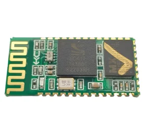
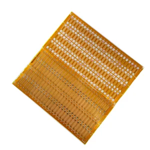
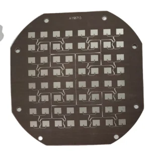


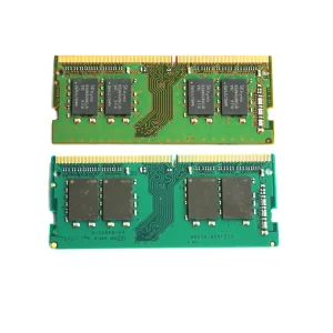
In the rapidly changing landscape of global electronics manufacturing, printed circuit boards (PCBs) represent the foundational architecture upon which modern digitalization is built. While high-density interconnect (HDI) boards and multi-layer configurations often dominate discussions concerning consumer smart devices, the global industrial economy continues to rely immensely on Single-Sided and Double-Sided PCBs. These components form the robust, reliable, and cost-effective backbone of systems ranging from power distribution networks and automotive control assemblies to heavy industrial machinery and high-sensitivity detection instruments.
Single-sided PCBs contain a single layer of conductive material (typically copper) on a non-conductive substrate. Their simplicity represents their primary advantage: they are highly cost-efficient, straightforward to manufacture, and yield exceptionally low error rates under high-volume production. Conversely, Double-sided PCBs extend this layout with dual conductive surfaces separated by an insulating layer, using plated through-holes (vias) to route signals across both the top and bottom traces. This architectural progression allows designers to achieve significantly higher component densities, tighter trace routing, and superior signal shielding without the cost multiplier of multi-layer manufacturing processes.
Rather than becoming obsolete, single- and double-sided boards have undergone a materials science revolution. Modern applications demand substrate variations that can withstand intense physical, electrical, and thermal stresses. The incorporation of advanced laminates like Taconic TLY-5 (0.254mm) and ceramic-filled PTFE substrates has propelled these fundamental form factors into high-frequency RF transmission systems and high-power LED installations, offering the structural integrity and thermal management critical for modern system reliability.
Procurement departments of multinational enterprises face increasingly complex challenges in selecting and vetting PCB factories and exporters. The decision-making framework is no longer restricted to cost-per-square-inch; instead, supply chain resilience, compliance certifications, testing thoroughness, and dynamic engineering support have emerged as primary sourcing criteria.
Global system integrators and OEMs seek partners who offer detailed documentation at every stage of the lifecycle. Key considerations include compliance with international regulatory frameworks such as UL 796 (for safety of printed wiring boards), IPC-A-600 Class II/III (acceptability of printed boards), RoHS (Restriction of Hazardous Substances), and REACH. Furthermore, in demanding environments such as automotive under-the-hood systems or industrial welding units, the reliability of solder mask thickness, trace width tolerances, and surface plating quality directly dictates the operational life of the final product.
Sourcing engineers require verified compliance with IPC-A-600 standards. Solderability, dielectric strength, and peel strength of copper foils are verified through automated optical inspection (AOI) and micro-section analysis.
Global enterprises mandate transparent supply paths. Sourcing from accredited laminators like Rogers, Taconic, or Shengyi ensures that base substrates meet strict halogen-free and eco-compliance requirements.
Procuring bare boards alone introduces assembly risks. Modern manufacturers offer integrated PCB Assembly (PCBA) services, mounting complex chipsets and testing the system end-to-end.
A testament to China's Smart Manufacturing 4.0: Leading the industry with high-precision PCB integration, advanced SMT assembly lines, and global export solutions.
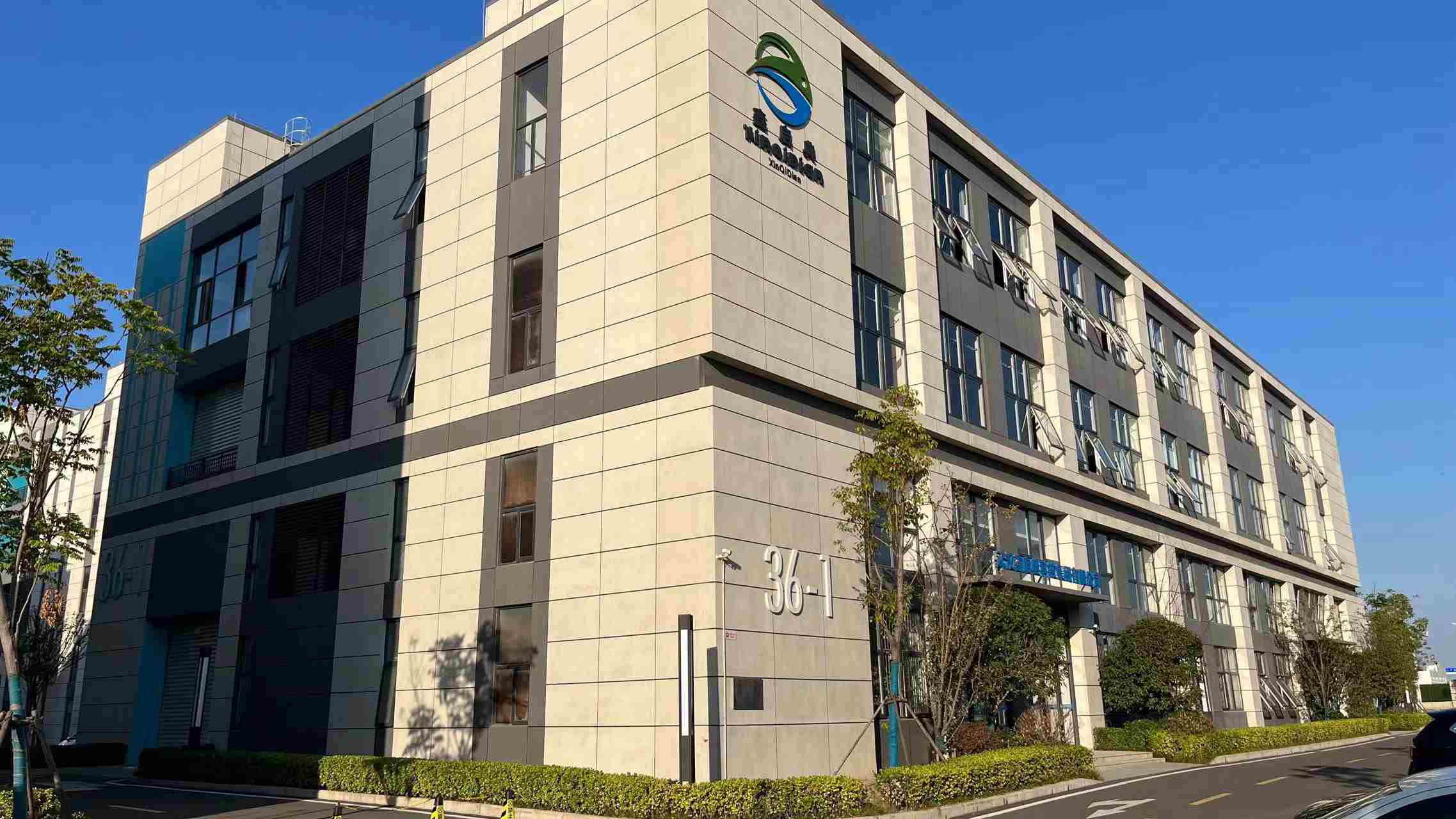
Founded in 2016, Corexis Memory Technology Co., Ltd. has established itself as an industry leader in manufacturing high-precision DDR5 and DDR4 memory modules, alongside advanced PCB design and assembly services. By combining 10 years of intensive electronic manufacturing experience with a state-of-the-art 21,800 m² facility, Corexis satisfies the rigorous engineering expectations of global OEMs, ODMs, and brand system integrators.
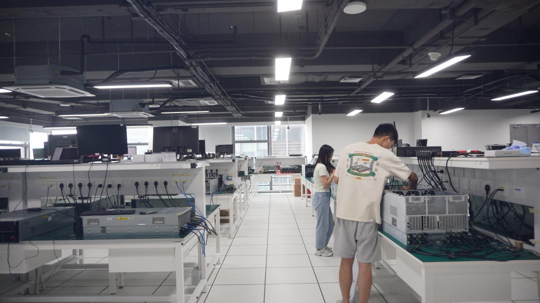
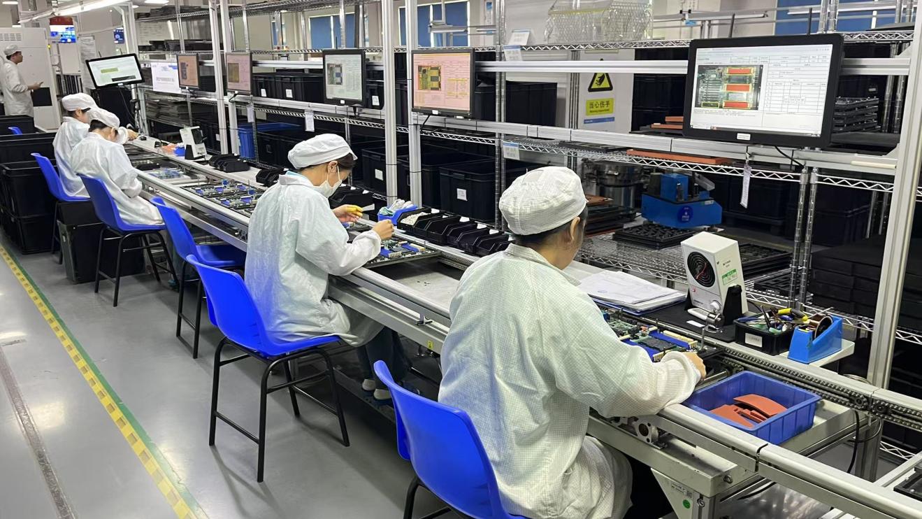
Our manufacturing ecosystem features cutting-edge Surface Mount Technology (SMT) lines and high-precision testing apparatus capable of routing, printing, and assembling components on demanding high-frequency substrates. Whether manufacturing specialized single-sided high-sensitivity PCB assemblies or double-sided multi-functional systems, Corexis integrates raw board fabrication, mechanical drilling, precision etching, component mounting, and robust quality verification workflows under a unified, quality-driven framework.
With a dedicated team of 56 QC specialists, the company maintains a rigorous inspection regime including:
In modern electronic systems, selecting the appropriate board material represents a critical design decision. Advanced applications can no longer rely solely on standard FR-4 laminates when thermal dissipation or signal losses present limiting design constraints. Below, we examine the primary material classes utilized in high-performance single- and double-sided PCBs:
| Substrate Type | Thermal Conductivity (W/m·K) | Dielectric Constant (Dk @ 1GHz) | Common Industrial Applications |
|---|---|---|---|
| FR-4 Standard | 0.25 - 0.4 | 4.2 - 4.8 | General consumer goods, basic control circuits |
| Aluminum Substrates | 1.0 - 4.0 | N/A (Metal Base) | High-power LED arrays, power supply units, motor drives |
| Taconic TLY-5 (PTFE) | 0.22 | 2.2 | High-frequency RF, microwave systems, radar modules |
| Rogers RO4003C / RO4350B | 0.62 - 0.64 | 3.38 - 3.48 | Automotive radar, cell base stations, satellite communications |
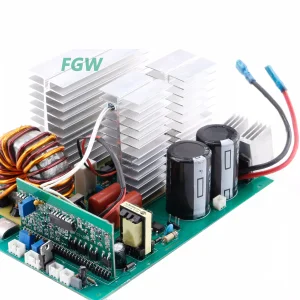
In designing a high-yield single-sided board, the routing path remains two-dimensional. Circuit patterns must not intersect; this demands clean mechanical planning, precise track routing, and the occasional use of jumper links. This architecture is optimal for low-frequency applications like welding motherboards (e.g., the ZX7-200/250 welding machine motherboards), where wide paths are necessary to accommodate high current densities without catastrophic thermal build-up.
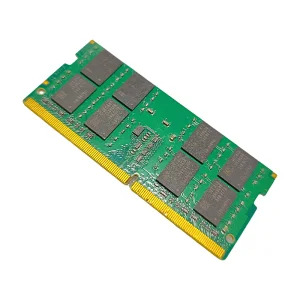
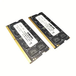
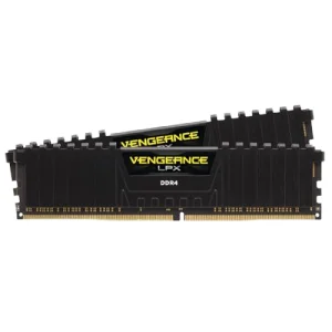
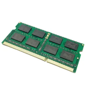
For double-sided layouts, the design paradigm relies on vias. When designing double-sided boards for RF or high-speed data transmission (such as Fury SAMBOWL laptop RAM or high-performance desktop memory sticks), designers must minimize parasitic inductance caused by through-hole transitions. Transitioning signals between layers introduces physical path anomalies that alter the line's characteristic impedance. Correct board design maintains a continuous return path underneath the signals, often utilizing the opposite side of the board as a solid copper ground plane to shield traces and prevent EMI (Electro-Magnetic Interference).
The global electronics supply chain demands dynamic adaptability. Chinese manufacturing centers have transitioned from traditional manufacturing hubs into advanced Industry 4.0 ecosystems. Factories leverage automation, MES (Manufacturing Execution Systems) software, and predictive logistical coordination to mitigate rising component and labor costs.
At Corexis's modern factory in Shenzhen, this efficiency translates into an integrated process. Modern SMT equipment places components at speeds up to 100,000 components per hour (CPH) with laser placement alignment. Quality checks are integrated at every key stage:
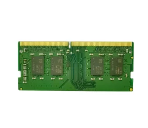
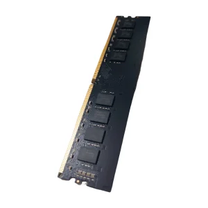
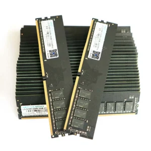
This level of control ensures that system components like memory modules (DDR4 16GB, 8GB, 4GB variants running from 1600MHz to 3200MHz) achieve consistent reliability, preventing infant mortality in field-deployed equipment.
Understanding user intent and application scenarios allows us to design and source circuit boards optimized for their operational environments:
Metal detection systems rely on the detection of minute phase shifts in electromagnetically coupled coils. Standard PCBs can introduce parasitic capacitances that drift with ambient temperature, leading to sensor inaccuracies. Using specialized double-sided PCB designs with precise trace widths and guard rings stabilizes the analog detection path.
By isolating the analog detector stage from noisy digital feedback lines on a single double-sided assembly, designers achieve higher sensitivity and stability, minimizing signal degradation across varied environments.
In arc welding machines, motherboards operate under harsh conditions characterized by high input voltages, thermal variation, and strong magnetic fields. The single-sided motherboard design is preferred here to simplify trace management and minimize interlayer arcing risk.
By designing heavy copper traces (typically 2oz or 3oz thickness) on a rigid FR-4 or ceramic substrate, these motherboards handle sustained currents, ensuring stable performance during continuous welding operations.
Get answers to the most common questions regarding PCB design, procurement, and advanced electronic engineering.
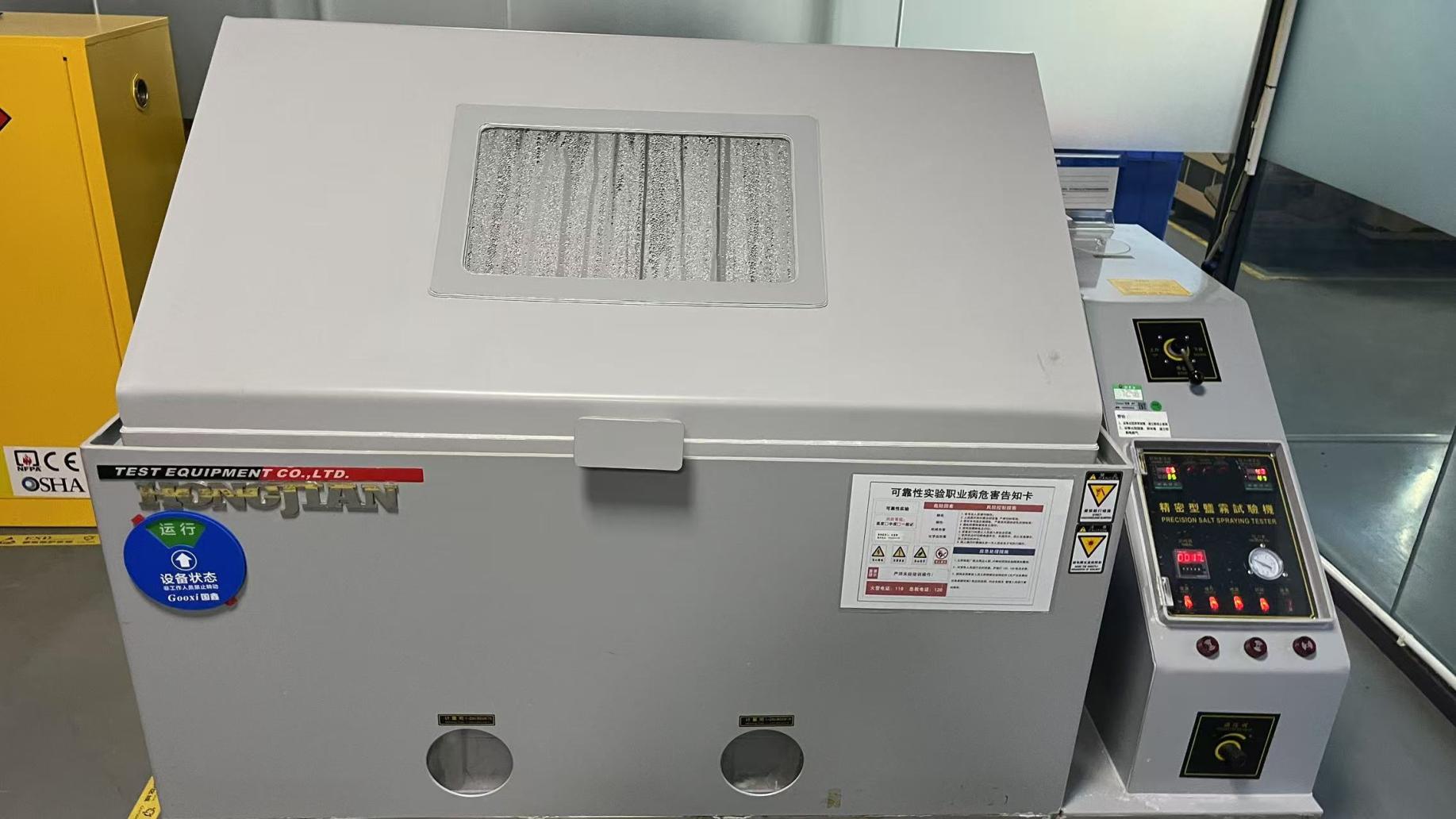
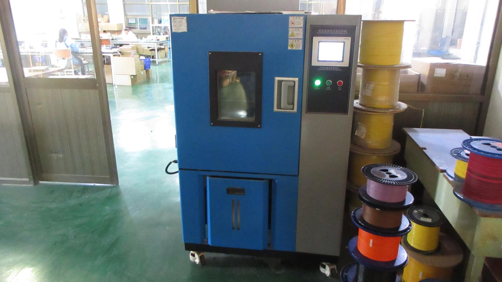
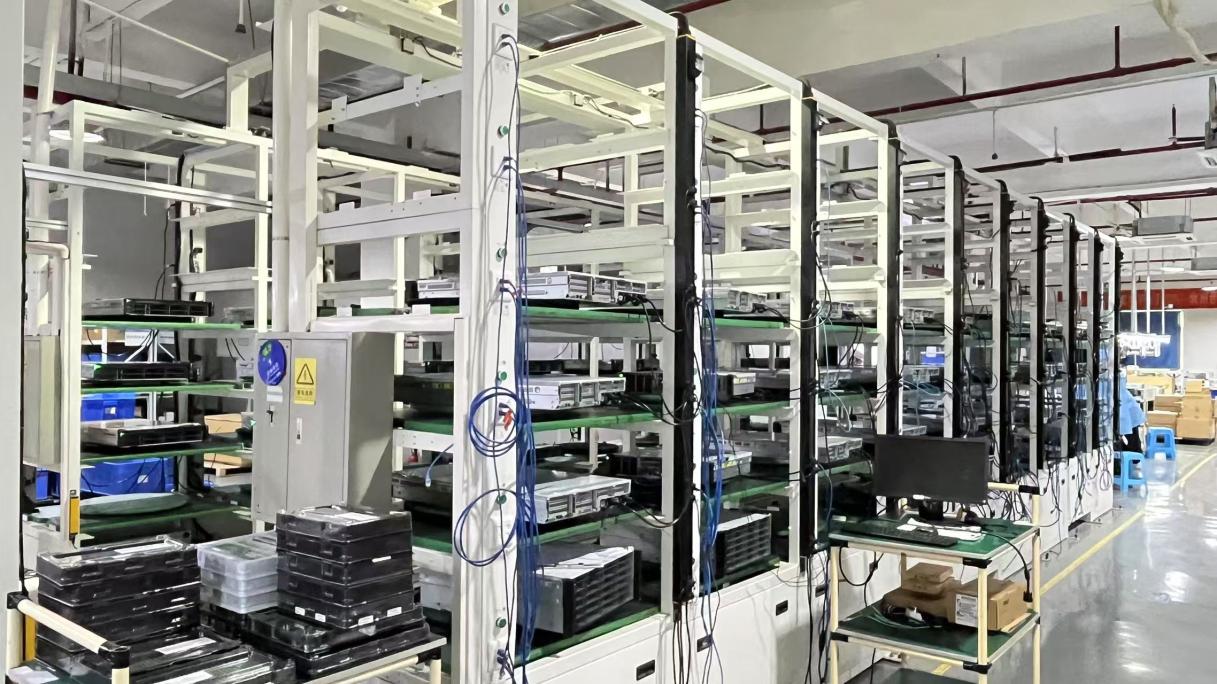
A visual tour of our production facility, showcasing SMT lines, quality inspection stations, and precision manufacturing capabilities.

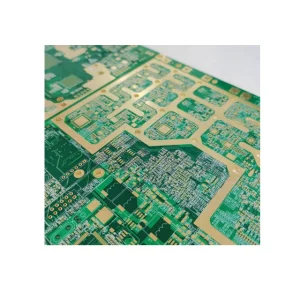
Complete system integration relies on selecting the appropriate components. Browse our range of high-frequency PCBs and high-capacity memory products below.
 Corexis Memory