High-Reliability Quick-Turn & Production-Run PCB Solutions for Southern California's Aerospace, Defense, Medical Device, and EV Industries.
Premium single and double-sided substrates engineered to fulfill quick-turn fabrication demands across the Greater Los Angeles metropolitan hub.
The Greater Los Angeles Area remains a premier hub for global technology innovation, spanning El Segundo’s aerospace corridor, Pasadena’s robotic and space laboratories, and Irvine’s medical device and EV automotive clusters. Navigating this dense industrial ecosystem requires a PCB manufacturing partner who understands that board reliability is not optional. From localized rapid prototyping to high-volume commercial production, the demand for high-integrity single-sided and double-sided Printed Circuit Boards (PCBs) is expanding rapidly.
In aerospace and defense, engineering groups demand compliance with IPC Class 3 standards, where double-sided boards must withstand severe thermal cycling and mechanical vibration. Meanwhile, medical device manufacturers in Southern California require highly specialized materials—such as bio-compatible polyimide substrates or ultra-thin flexible circuits—to fit miniaturized diagnostic enclosures. As a premier manufacturer serving the Los Angeles region, we bridge the gap between fast-turn localized engineering iterations and robust global volume scaling.
To optimize an electronics program for cost, performance, and manufacturability, hardware teams must analyze the trade-offs between single-sided and double-sided architectures. Below, we break down key differences in material, layout complexity, and heat dissipation:
| Feature Parameter | Single-Sided PCBs | Double-Sided PCBs |
|---|---|---|
| Typical Substrates | FR-4, CEM-1, CEM-3, FR-1, Aluminum-Clad | FR-4 High-Tg, Taconic, Rogers, Polyimide |
| Copper Layer Count | 1 Layer (Single Outer Face) | 2 Layers (Top and Bottom Outer Faces) |
| Interconnections | No vias required; component-to-trace direct mounting | Plated Through-Holes (PTH) and Micro-vias |
| Routing Density | Low; simple schematic traces without crossovers | Moderate to High; complex crisscross trace paths |
| Best Applications | Power supplies, LED boards, simple industrial sensors | High-speed controllers, RF communications, power amps |
| Thermal Performance | Excellent with metal-clad/aluminum bases | Excellent via thermal arrays and multi-layer paths |
Single-sided PCBs provide the ideal path for high-power thermal management (especially with metal-clad/aluminum cores), because the heat-generating components are mounted directly on one side, allowing the solid aluminum substrate below to channel heat efficiently away from sensitive parts. Double-sided PCBs, by contrast, utilize Plated Through Holes (PTH) to route signals across two conductive copper planes, which enables more compact layouts, integrated shield layers, and complex analog-digital component isolation.
A global leader in DRAM, high-speed SMT assembly, and rigid-flex PCB fabrication serving OEMs, ODMs, and industrial brands since 2016.
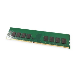
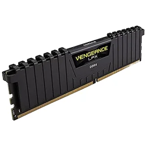
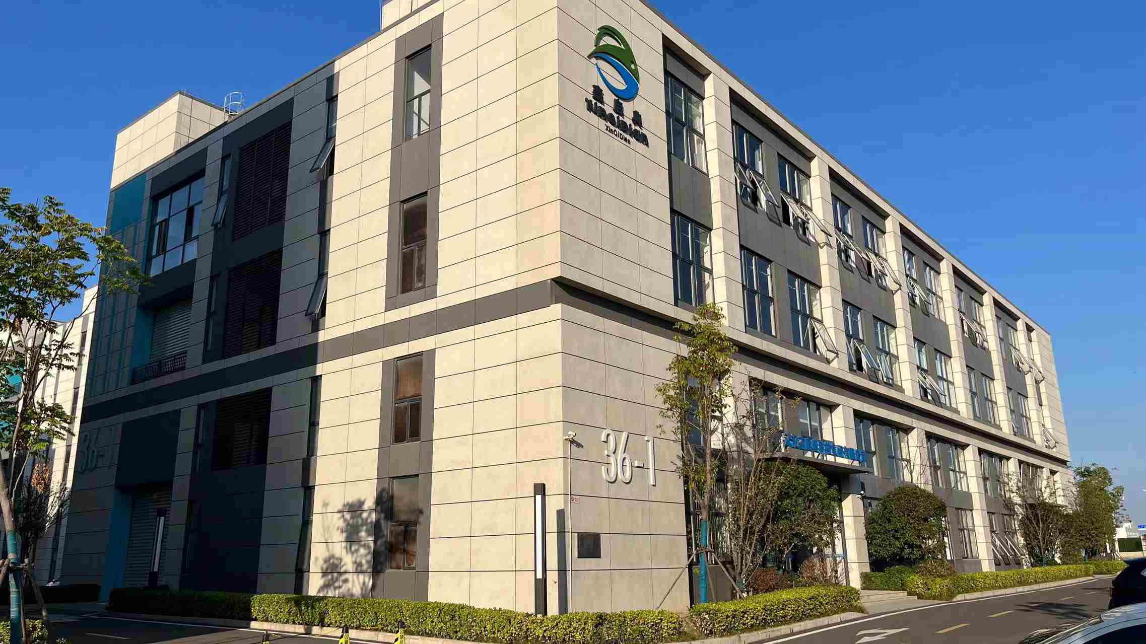
Corexis Memory Technology Co., Ltd. is a highly specialized electronics manufacturer and exporter dedicated to delivering high-performance DRAM modules and complex PCB solutions. Established in 2016, the company integrates advanced SMT processing, custom PCB fabrication, and component-level testing under a unified quality assurance protocol. Our high-capacity manufacturing footprint and strict engineering standards enable us to deliver ruggedized boards and memory subsystems to industrial partners worldwide, including defense, aerospace, and medical system integrators in Los Angeles and the broader North American market.
Our facility runs multiple state-of-the-art SMT lines featuring high-speed Yamaha and Fuji pick-and-place systems, in-line 3D SPI (Solder Paste Inspection), AOI (Automated Optical Inspection), and real-time X-ray monitoring. By controlling both the PCB fabrication and the high-speed chip placement phases, we guarantee exceptional reliability for critical signal-integrity components, including DDR5 memory boards, RF communication control boards, and multi-layer microcontrollers.
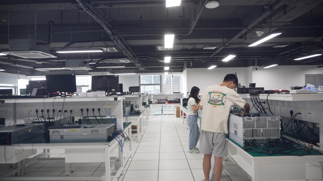
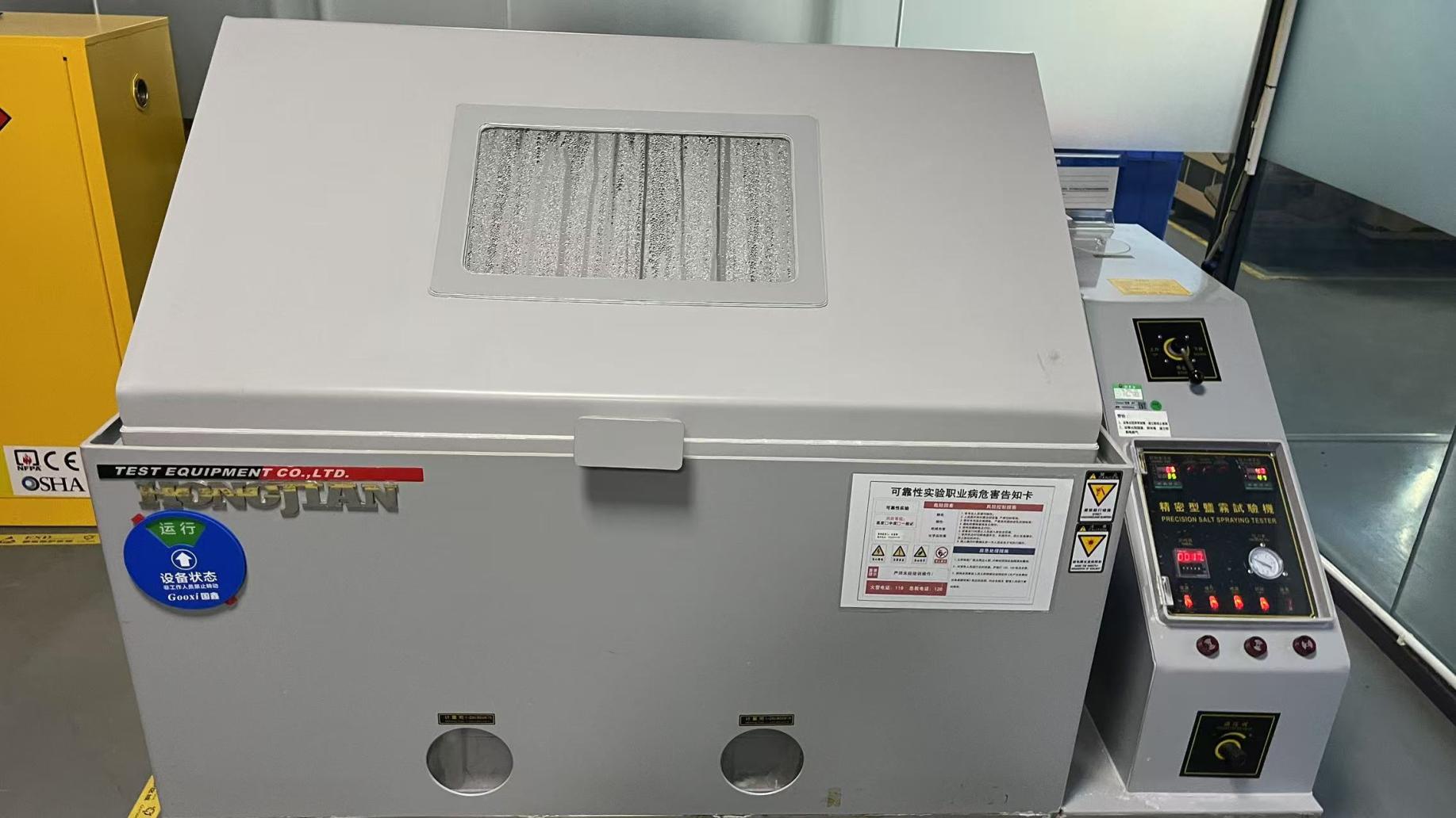
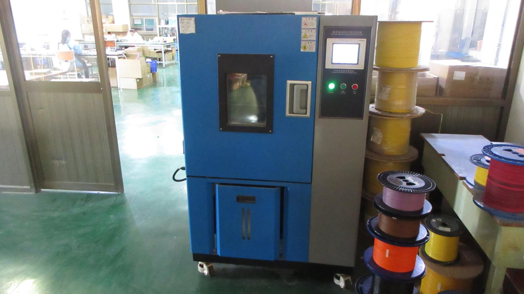

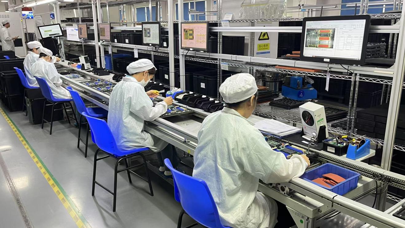
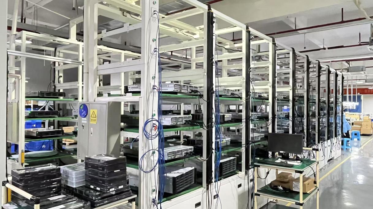
To support critical applications in LA aerospace, defense, and healthcare, we apply a multi-tier Quality Assurance protocol. Our 56-strong quality control staff tracks every board from copper laminate incoming verification to final electrical packaging:
We source raw laminates exclusively from globally recognized material suppliers (including Shengyi, Rogers, Isola, and Taconic). Trace copper weight and substrate dielectric thickness are verified via spectrophotometry and micro-sectioning before entering production.
Using laser-guided automated optical scanning and chemical concentration analysis in the plating baths, we verify trace-width precision, registration alignment, and plated through-hole wall copper thickness in real-time. This reduces defects before solder mask application.
Every single-sided and double-sided board undergoes 100% Electrical Testing (via flying probe or dedicated test fixture) to confirm electrical continuity and isolation. Cross-section analysis, solderability tests, and thermal stress tests are conducted on test coupons to ensure the laminates will not delaminate under intense SMT reflow profile cycles.
The global PCB market is shifting rapidly toward higher performance, improved thermal dissipation, and tighter environmental compliance. Below are the key technological forces driving engineering decisions in Southern California:
As electric automotive designs (including EV battery management systems and power converters developed in Irvine and Torrance) demand higher current density, standard FR-4 substrates fall short. We utilize high-thermal-conductivity metal substrates (such as copper or aluminum bases with ceramic-filled dielectric layers) to achieve thermal conductivities of 1.0 W/m-K up to 8.0 W/m-K, ensuring efficient heat transfer and preventing component thermal runaway.
Aerospace telemetry and 5G transceiver modules require low dielectric constant (Dk) and low dissipation factor (Df) to minimize signal loss. By utilizing Taconic TLY-5 (Dk 2.2) and Rogers woven glass PTFE laminates in double-sided configurations, we deliver predictable impedance pathways for RF applications running in the gigahertz spectrum.
Aligning with California's stringent environmental mandates and global RoHS/REACH restrictions, our manufacturing lines supply halogen-free FR-4 options. These materials utilize phosphorus-based flame retardants that release non-toxic smoke in emergency events while maintaining high thermal glass transition temperatures (Tg > 170°C).
Explore our full range of double-sided boards, high-density development kits, and industrial-grade memory modules configured for global hardware ecosystems.
Clear, direct answers regarding lead times, material standards, capabilities, and global procurement procedures.
 Corexis Memory