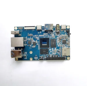
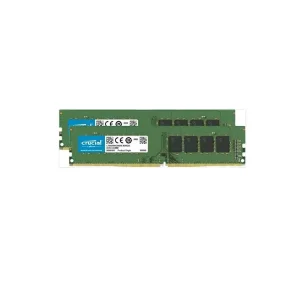
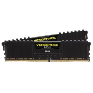
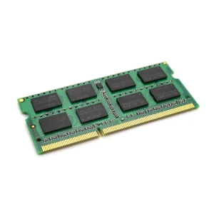
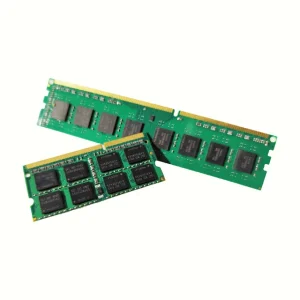
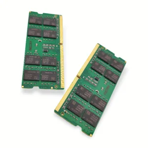
Explore our top-tier SMT-compatible modules, micro-machined hardware, and multi-layer PCBs manufactured under strict IPC standards.

The electronic manufacturing services (EMS) sector has transitioned into an era of unprecedented miniaturization. At the core of this transition lies the SMT (Surface Mount Technology) stencil, a precision-engineered tool designed to control the deposition of solder paste onto Printed Circuit Boards (PCBs). Globally, the laser-cutting stencil market has evolved from simple mechanical chemical-etching profiles to advanced, sub-micron laser micro-machining workflows.
Industrial demand shows that APAC, specifically China, acts as the global powerhouse for both SMT stencil fabrication and PCB assembly operations. The modern SMT lines in regions like North America and Europe rely heavily on premium stencils exported from China to support automotive control units, high-performance computing (HPC) motherboards, aerospace hardware, and medical electronics.
By leveraging advanced laser systems, Chinese factories achieve aperture positional tolerances of less than ±2μm, satisfying the exacting standards of fine-pitch components such as 01005 passives and 0.3mm pitch BGAs (Ball Grid Arrays). The focus is no longer just on cutting through stainless steel sheets; it centers on optimizing aperture wall roughness, wall draft angles, and post-cutting chemical polishing to ensure perfect solder paste release.
As components shrink, the materials, geometry, and surface finishes of laser cutting stencils must evolve to avoid paste bridging, insufficient paste, and costly board reworks.
Standard SUS304 steel is replaced by fine-grain and ultra-fine-grain alloys (grain size < 5μm). This specialized molecular structure yields smoother laser-cut walls, uniform heat dissipation during cutting, and reduces micro-cracking at the aperture boundaries.
Dual-layer hydrophobic and fluxphobic nano-coatings are applied via chemical vapor deposition (CVD). This reduces the required cleaning frequency of the stencil underside by up to 70%, increases yield, and ensures a cleaner paste release for micro-BGA components.
Integrating components of widely varying sizes on a single PCB requires step stencils. Through chemical etching or laser milling, localized regions of the stencil are thinned (step-down) or thickened (step-up) to deposit precise volumes of solder paste.
Our engineering expertise and massive factory infrastructure empower us to supply premium stencils and memory modules globally with absolute quality control.
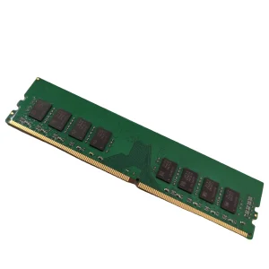
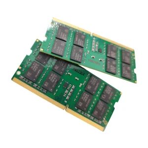
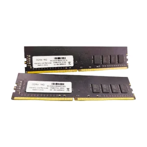
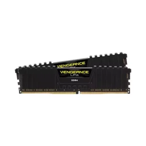
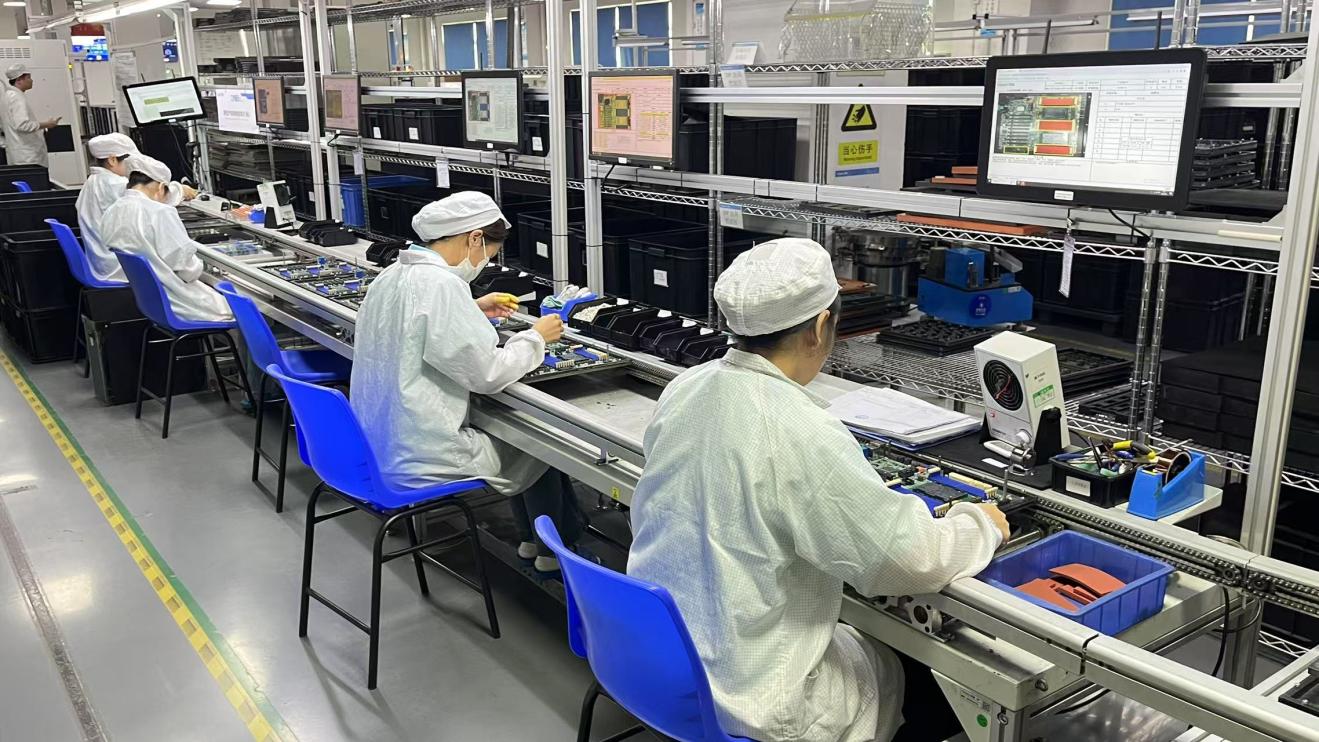
Established in 2016, Corexis Memory Technology Co., Ltd. has grown into a premier manufacturer of high-performance DRAM solutions, serving the global SMT, OEM, and ODM sectors. While we design and manufacture high-density DDR4 and DDR5 memory modules for servers, laptops, and desktop systems, our core manufacturing advantage stems from our state-of-the-art SMT lines.
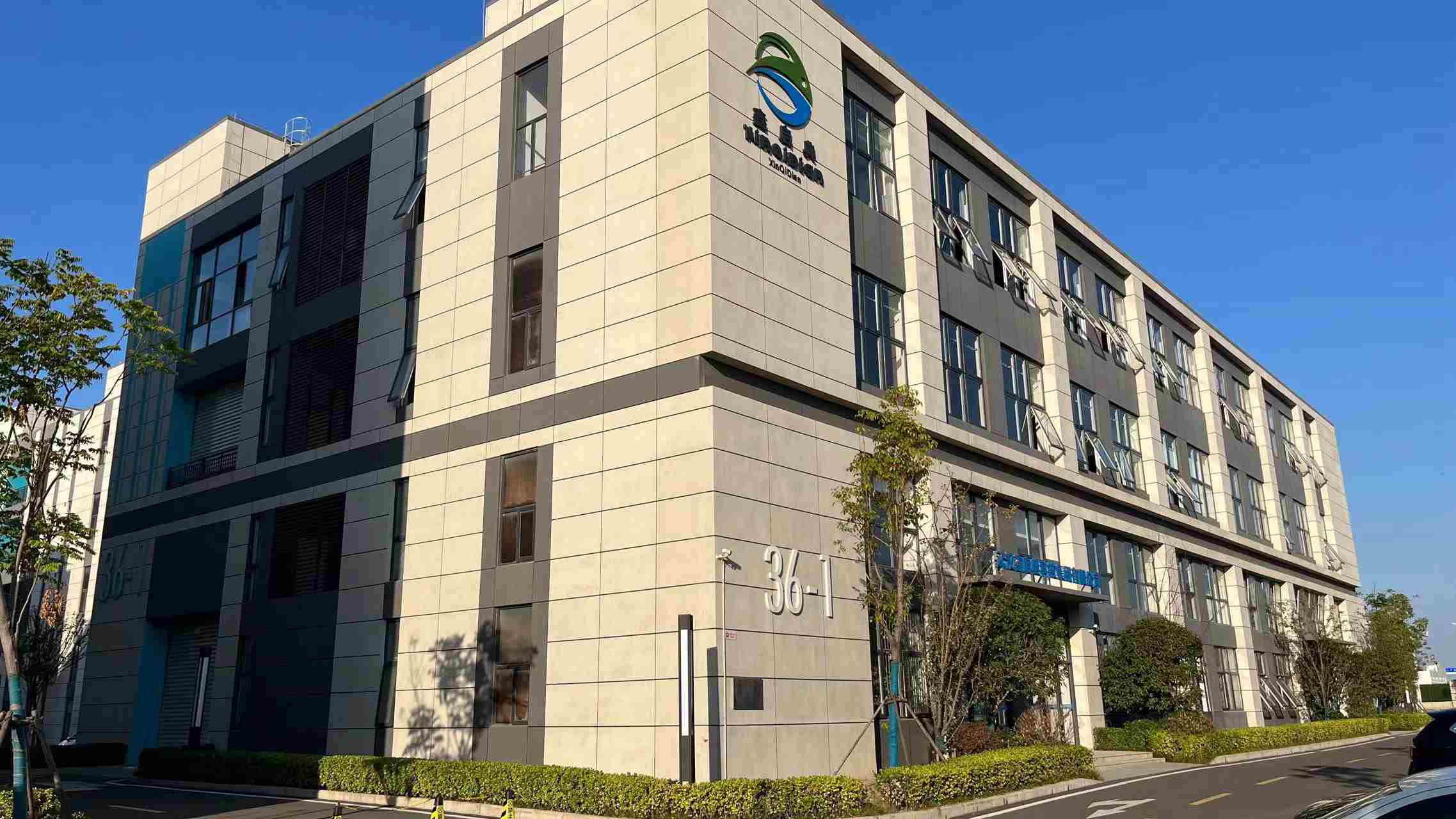
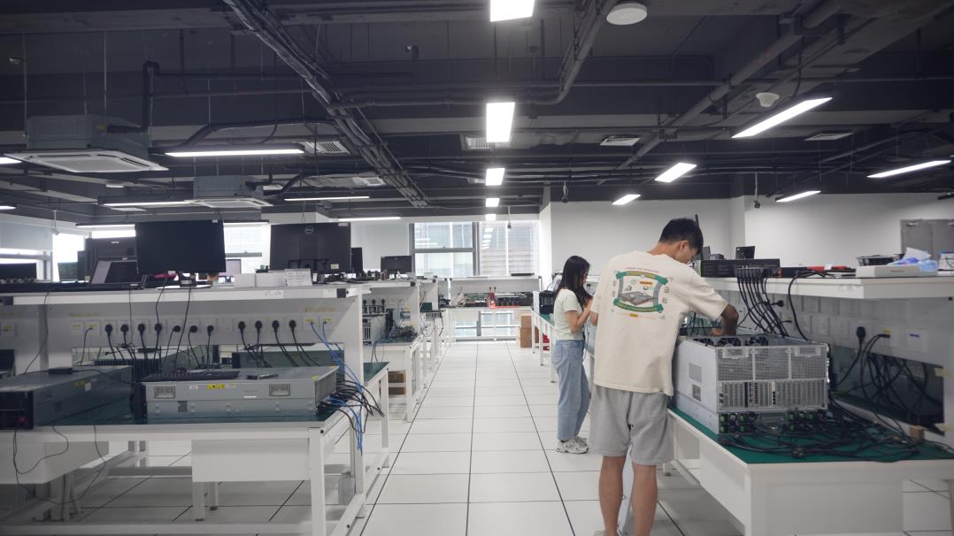
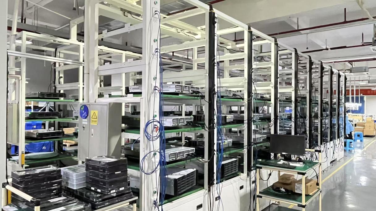
We leverage our internal deep-level understanding of SMT precision engineering to produce and export industrial-grade Laser Cutting Stencils. Because we operate high-precision pick-and-place lines daily, we understand the exact tolerances required for stencil apertures, tension parameters, and substrate-level gaskets. Our 21,800 m² factory integrates R&D, SMT production, laser stencil fabrication, packaging, and QA under one roof to deliver unmatched reliability.
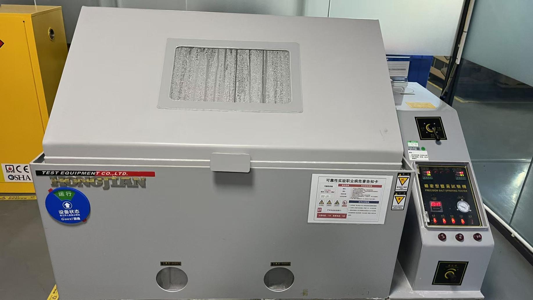
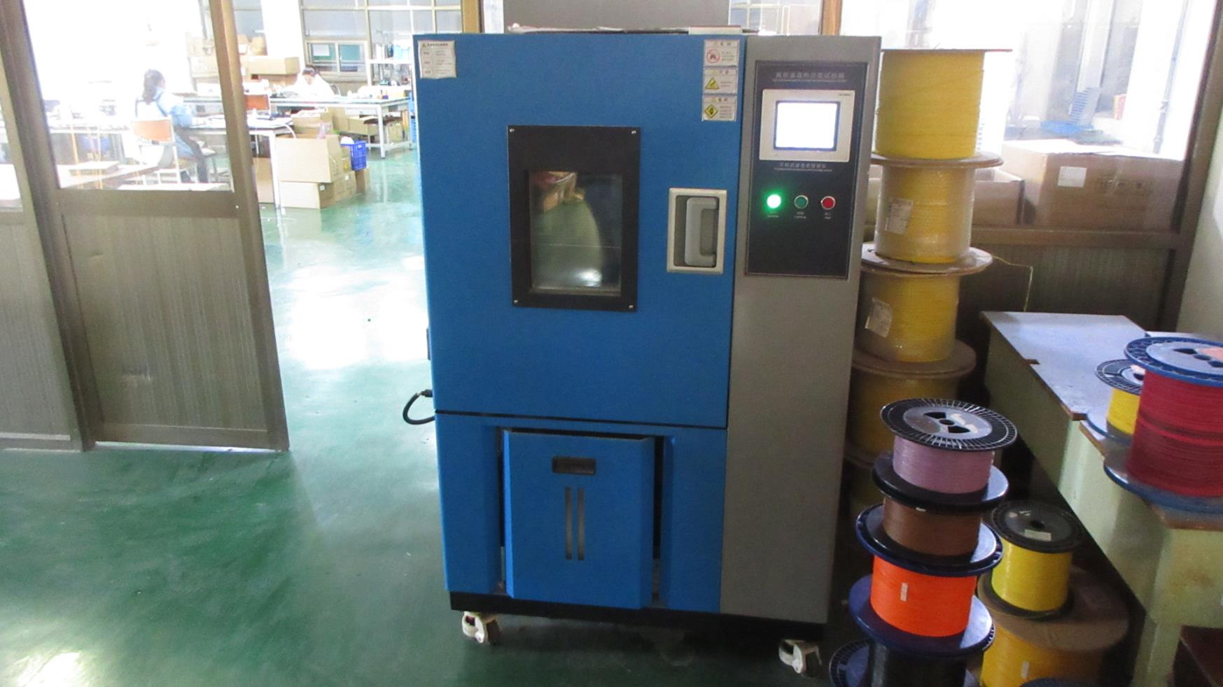
Corexis partners with over 1,120+ supply chain networks worldwide. We provide custom solutions for brand owners, system integrators, industrial computer manufacturers, and contract distributors. Our products undergo rigorous testing processes, including incoming material inspection (IQC), in-process inspection (IPQC), final quality control (FQC), and reliability/compatibility testing.

Our high-precision stencils and assemblies are custom-designed for a broad spectrum of industrial environments.
Automotive components demand zero-defect performance. Stencils must feature smooth, tapered aperture walls to guarantee consistent solder volume for critical components like ADAS controllers, power inverters, and battery management systems (BMS).
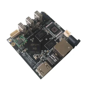
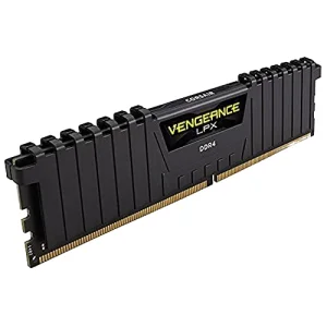
Server memory modules utilize tiny, fine-pitch CSP/BGA layouts. Our specialized electro-polished and nano-coated stencils ensure clean solder releases, preventing bridges between contacts and eliminating costly manual board cleanups.
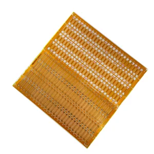
For miniaturized wearables, flex-circuit (FPC) keyboards, and multi-layer micro-controllers, our step-down stencils deliver different solder volumes to different parts of the same board in one clean squeegee stroke.
Solder paste printing is responsible for up to 70% of all SMT defects. Choosing the correct wholesale laser cutting stencil factory is a critical step in avoiding common SMT assembly issues, such as solder bridging, voiding, and insufficient wetting. When selecting a manufacturing partner, assembly engineers must pay close attention to three primary criteria: material composition, aperture engineering, and structural tensioning.
The layout design of stencil apertures directly impacts transfer efficiency—the ratio of the volume of printed solder paste to the design volume of the aperture. Laser-cutting technology allows for minor draft angles (tapered aperture walls), typically 1 to 2 degrees, with the opening on the PCB side being slightly larger than the squeegee side. This trapezoidal geometry facilitates an unhindered paste release as the PCB moves downward after printing.
Modern factories utilize fiber laser systems rather than legacy CO2 systems. Fiber lasers feature a highly concentrated beam diameter (typically 20μm or smaller) and high energy density, allowing them to cut stainless steel with minimal heat-affected zones (HAZ). This leaves clean edges, eliminating micro-burrs and slag buildup that can cause the stencil to sit unevenly on the PCB during print cycles.
Shipping custom stencils globally requires specialized protective frames and vacuum packaging. Our logistics division handles worldwide delivery, using reinforced aluminum frame packing and moisture-barrier protective bags. We match your production schedule with short lead times, ensuring custom laser-cut stencils reach your SMT facility within days of design approval.
Get answers to the most common questions regarding laser-cut stencils, SMT processing, and wholesale custom options.
Wholesale memory modules, custom PCB designs, and cooling solutions built to power next-generation computing systems.

 Corexis Memory