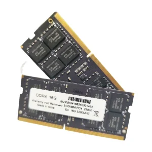
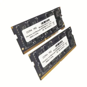
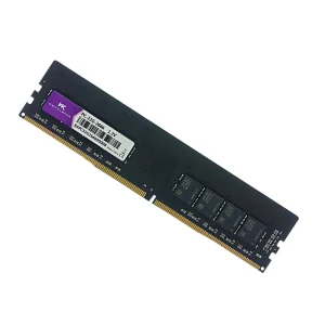
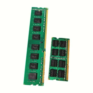
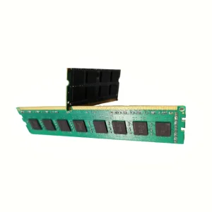
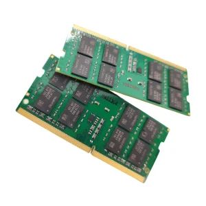
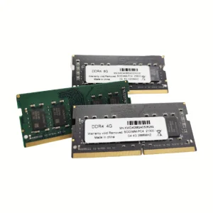
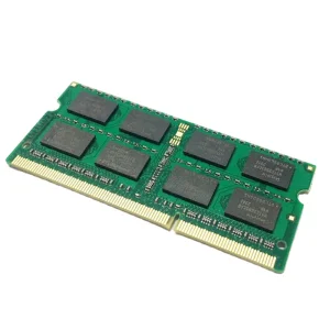
Discover our primary line of high-performance components designed to support fast-cycle prototyping and scalable production runs.

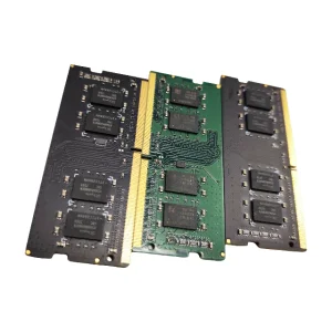
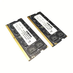
Bridging high-precision manufacturing with local engineering specifications to power Europe's leading industrial corridor.
Milan serves as the central node for Italy's advanced manufacturing and industrial design sectors. With the region transitioning aggressively toward IoT-enabled automation, there is an surging requirement for multi-layer PCBs that support high thermal stability, high frequency, and miniature layouts. Our operations directly address these needs with specialized fast-track prototyping channels for Milanese engineering consultancies and production plants.
The global microelectronics market requires unprecedented supply resilience and strict compliance with design-for-manufacturability (DFM) rules. As an experienced exporter, Corexis bridges local European operations with robust global resource networks. We minimize components lead times by keeping safety stock of critical raw laminates, such as Rogers and high-Tg FR-4, mitigating macro-level supply disruptions.
From smart grids and automotive telematics systems in the Lombardy district to high-reliability computing servers based in northern Milan data centers, our high-density, multi-layer circuit boards provide the mechanical and electrical integrity needed to resist extreme vibration, thermal cycles, and signal degradation over long operational lifespans.
An established OEM/ODM leader with deep engineering capabilities and 100% full-inspection quality control systems.
Corexis Memory Technology Co., Ltd. is a professional DDR5 memory and advanced PCB systems manufacturer dedicated to delivering high-performance DRAM and multilayer circuit solutions for global OEM, ODM, and brand customers. Since our establishment in 2016, we have focused on memory technology innovation, advanced SMT manufacturing, and strict quality management. Our products are widely used in desktop PCs, laptops, servers, industrial computers, embedded systems, and AI applications.
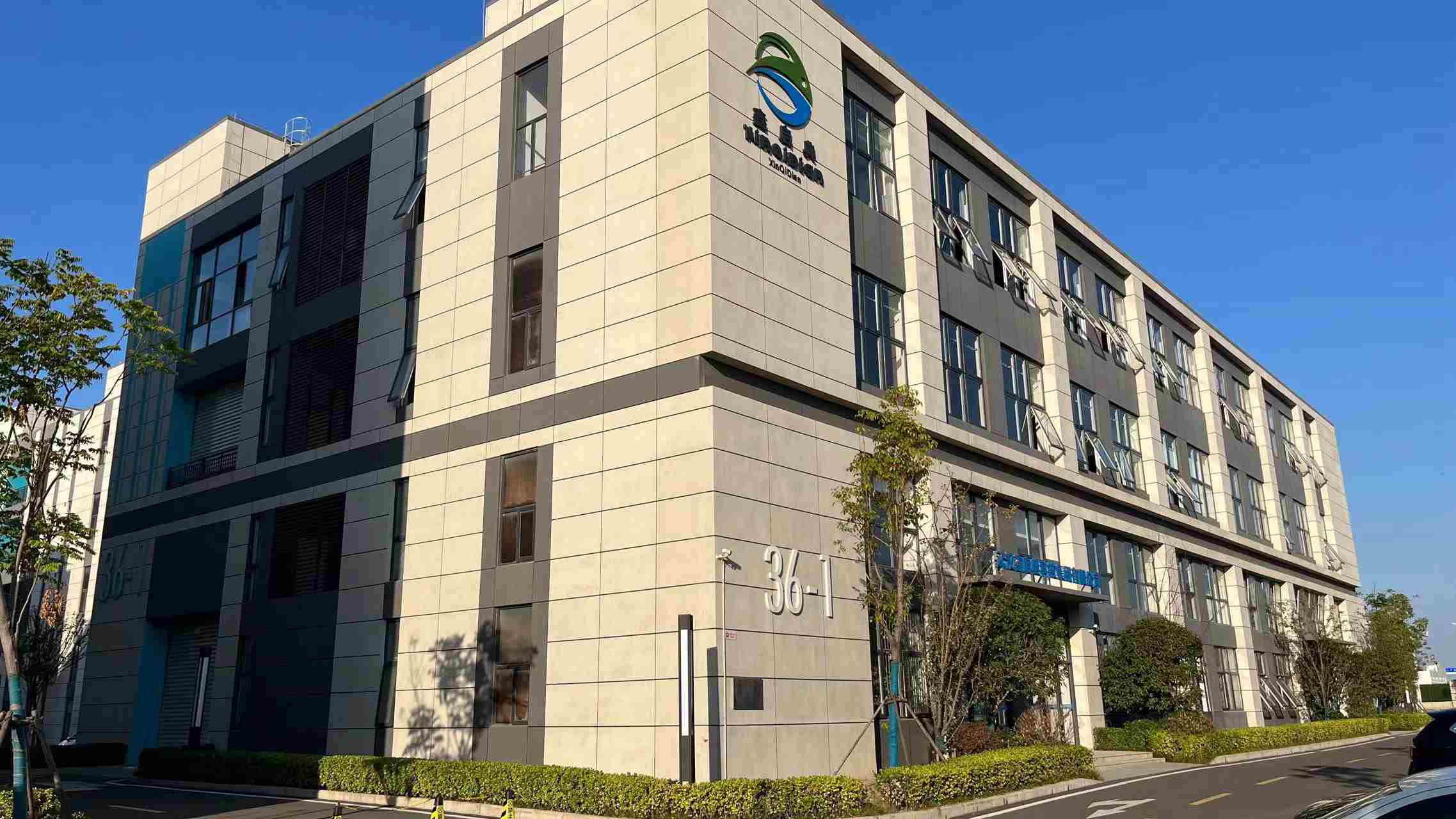
With a modern manufacturing facility covering 21,800 m², Corexis integrates R&D, SMT production, testing, packaging, and quality assurance under one roof. Our experienced engineering team continuously develops reliable and high-speed memory products and multilayer PCBs that meet strict international standards and the evolving demands of the global market.
Ensuring your components meet European Union directives, quality metrics, and future technical roadmap milestones.
We supply PCBs that align with CE, RoHS, and WEEE directives, guaranteeing clean, hazard-free materials suitable for direct distribution in Italy and the wider European market. All designs go through localized DFM reviews to avoid post-order bottlenecks.
Supported by 56 dedicated Quality Control staff, we employ Incoming Material Inspection (IQC), In-Process Inspection (IPQC), Final Quality Control (FQC), Outgoing Quality Assurance (OQA), and compatibility testing protocols to prevent defects.
From custom copper weights (up to 6 oz for power electronics) to high-speed digital layups (over 32 layers), our system provides localized technical support, custom packaging design, capacity configuration, and customized heat spreaders.
| Parameter / Process | Capabilities & Range | Milan Market Standards Met |
|---|---|---|
| Layer Count Range | 2 to 32+ layers | High-density industrial Automation controllers |
| Base Materials | FR-4 (High-Tg), Rogers, Polyimide, Metal Core (MCPCB) | Automotive power-train and telematics systems |
| Finished Copper Thickness | 0.5 oz to 6 oz | High-current welding machine inverters & EV setups |
| Surface Finish Options | HASL, Lead-free HASL, ENIG, OSP, Hard Gold plating | High-durability medical & defense applications |
| Minimum Trace / Space | 0.075mm / 0.075mm (3mil / 3mil) | Compact handheld IoT designs & RAM controllers |
Our development trajectory aligned with emerging trends in IoT, 5G infrastructure, and AI hardware acceleration.
Scaling standard production capabilities to support microvia densities below 50 microns. This will allow next-generation wearables and medical IoT nodes in Northern Italy to package more computing power into ultra-thin profiles.
Integrating passive and active silicon components inside the inner layers of the PCB substrate itself to boost noise immunity, high frequency response, and thermal dissipation.
Formulating hybrid stack-ups featuring ultra-low-loss Teflon and advanced ceramic matrices designed specifically for the impending wave of smart city infrastructure and automated vehicle networks.
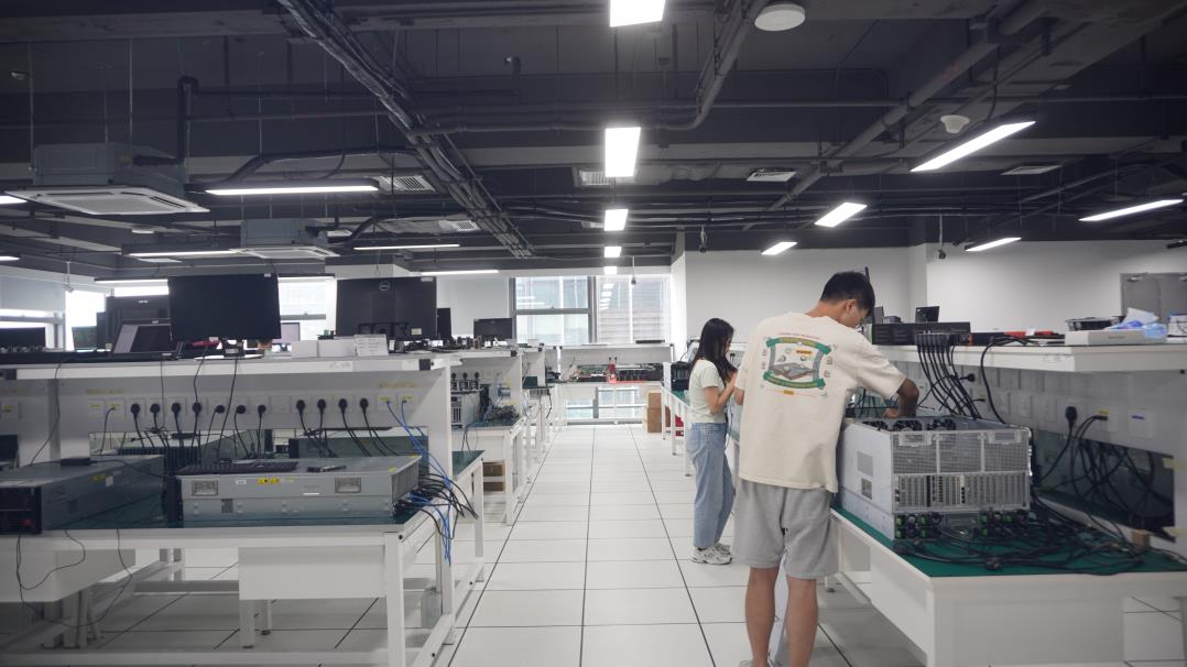
A glimpse inside our 21,800 m² cleanroom and advanced automated surface-mount assembly lines.
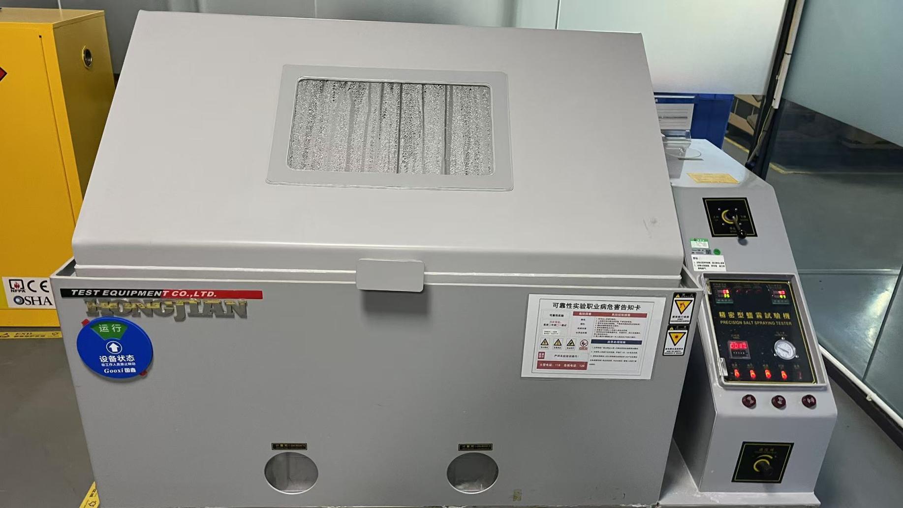
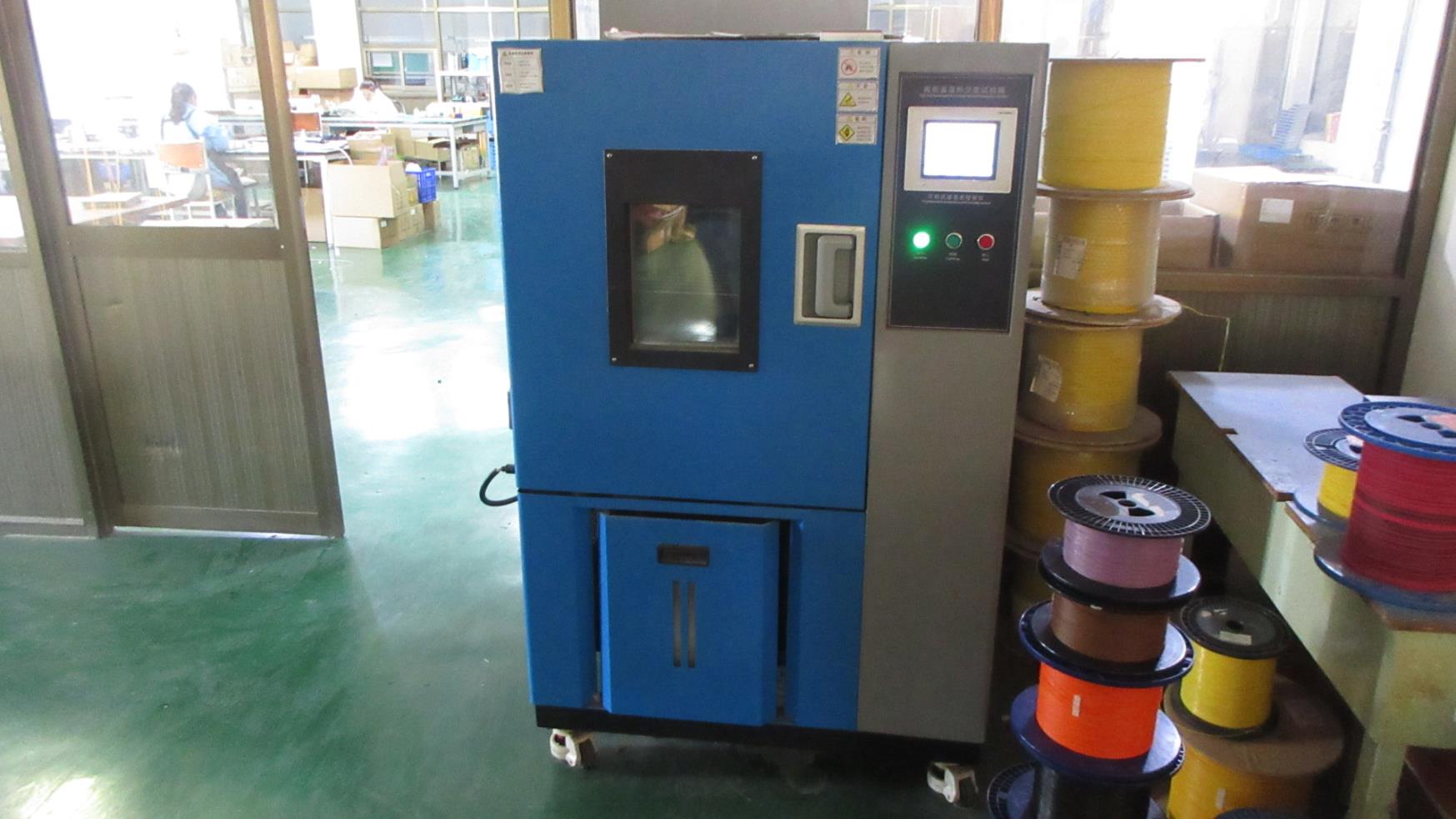

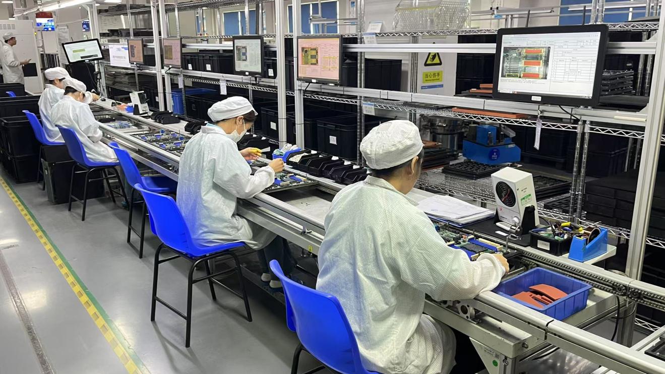
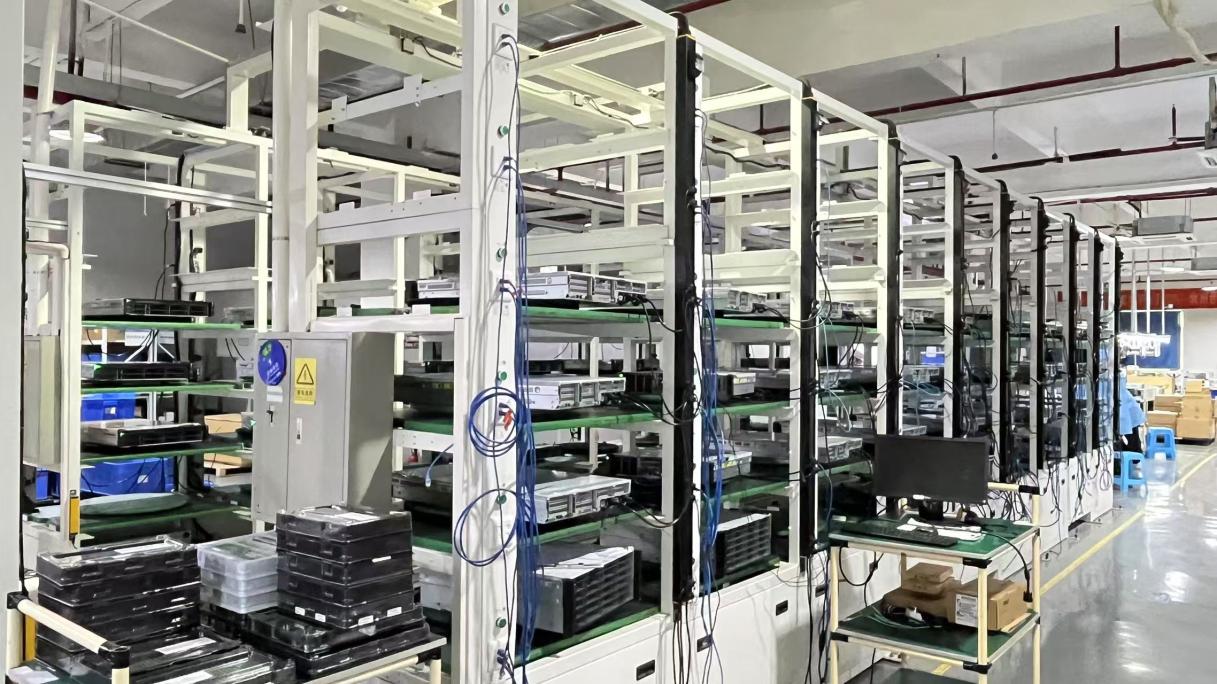
Our deep catalogue of high-speed memory modules, customized computer architectures, and high-frequency PCBs.

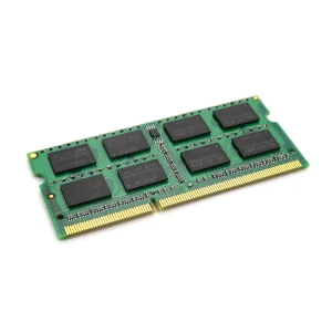
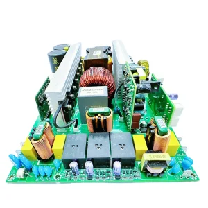
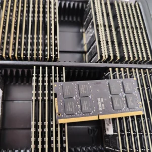
Quick engineering and supply chain references for our Milan and global enterprise customers.
A: Standard express shipping and custom clearance routes to Lombardy take approximately 5 to 7 working days. For urgent micro-batch prototypes, we leverage expedited carrier options.
A: Yes, our engineers perform structural and electrical DFM (Design for Manufacturability) inspections on all Gerber files to verify stack-up integrity, thermal routing, and component clearances.
A: Absolutely. All multilayer circuit boards and components shipped to European customers comply with REACH and RoHS standards, and are accompanied by full material data declarations.
A: We manufacture HDI boards up to 32 layers with blind/buried vias, microvias, laser drilling, and low-loss dielectric layers optimized for 5G communications and AI servers.
 Corexis Memory