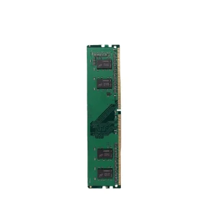
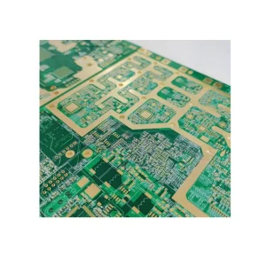
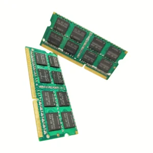
Top China Thick Copper Circuit Boards Manufacturer & Factories

Advanced High-Current Heavy Copper PCBs, Custom Power Electronics, and High-Speed Computing Substrates Formulated for Maximum Thermal Performance & Reliability.

Bridging Heavy Copper Technologies & Advanced System Integration

As industrial automation, high-power energy sectors, and advanced computing paradigms evolve, the demand for electronic assemblies capable of handling extreme current densities and thermal loads has surged. In this high-stakes technological arena, standard circuit boards fail to meet reliability limits. Thick Copper Circuit Boards (Heavy Copper PCBs), featuring copper weight ranges from 3 oz/ft² to over 20 oz/ft², have transitioned from niche components to fundamental necessities.

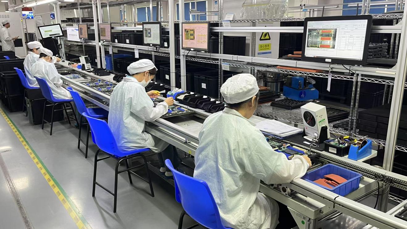
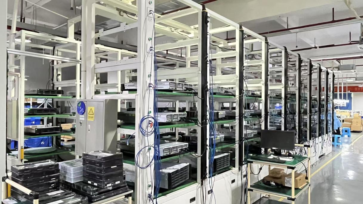
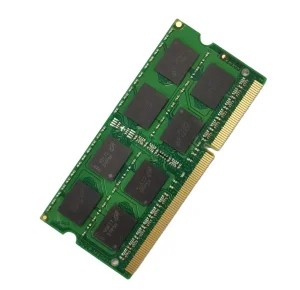
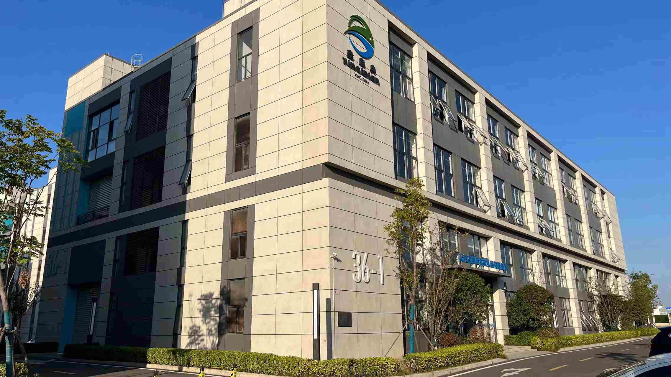
At the center of this electronic manufacturing paradigm is Corexis Memory Technology Co., Ltd. Established in 2016, our operation has scaled beyond its core identity as a professional DDR5 memory manufacturer. Leveraging a state-of-the-art 21,800 m² modern facility, Corexis fuses cutting-edge SMT production, hardware development, firmware optimization, and custom heavy-copper PCB design. This unified manufacturing capability allows system integrators and global OEM partners to secure robust electronic boards that display uncompromising stability under intense environmental stress.

Information Gain: Unlike conventional PCB manufacturers that separate bare-board fabrication from component assembly, a unified approach ensures that heavy copper boards are optimized for high-temperature reflow soldering, eliminating internal delamination risks before shipment.
2016
Established
21,800m²
Factory Area
128
R&D Engineers
1,120+
Supply Chain Partners

Industrial Core Profile & Technical Framework

Corexis combines specialized hardware engineering with rigorous manufacturing metrics to satisfy global procurement compliance.

Export Expertise
8 years of global export experience serving North America, Europe, Southeast Asia, South America, and the Middle East. Annual export revenue exceeds USD 26,800,000.
Rigorous Quality Systems
100% full inspection managed by 56 dedicated QA/QC specialists executing IQC, IPQC, FQC, OQA, and strict thermal validation.
Deep Customization
Private label, custom board outlines, heavy copper layer configurations, customized heat-spreader design, and full SMT component populating.
Agile R&D Architecture
128 R&D engineers driving rapid design iterations. Released 86 new product designs last year alone, focusing on signal integrity and heat dissipation.

Thick Copper Circuit Boards: Market Trends & Global Procurement Priorities

A professional exploration into high-current substrates, shifting dynamics, and thermal efficiency requirements.

1. The Rise of Heavy Copper in Energy and Transportation

The transition toward electrification has placed extreme demands on printed circuit boards. Standard PCB tracking layers (1 oz/35µm copper thickness) degrade when subjected to currents exceeding several amperes. Heavy copper boards (ranging from 3 oz to 20 oz or more) integrate thick conductors to sustain high currents without generating hazardous local temperature rises.

Key drivers include:

  • Electric Vehicles (EV) & Charging Infrastructure: Power converters, onboard chargers (OBC), and ultra-fast DC charging stations demand up to 400A peak currents. Heavy copper tracks prevent overheating, ensuring long-term system life.
  • Renewable Energy Systems: Solar inverters and wind power converters leverage thick copper to withstand fluctuating high voltages while minimizing heat buildup inside dense cabinet spaces.
  • AI Compute & Hyperscale Servers: Modern high-performance processors demand hundreds of watts per socket. Multi-layer hybrid PCBs—combining thick copper power cores with high-speed, high-frequency signal layers (such as Rogers 4000 or Shengyi High TG170)—are essential to optimize power delivery networks (PDN).

2. Sourcing Dilemmas & Purchasing Strategy

Global procurement directors face multiple bottlenecks when sourcing heavy copper PCBs from China. The primary concern is not just the raw copper cost, but the manufacturer's ability to maintain registration accuracy on thick layers, avoid resin starvation, and perform high-quality solder mask coverage over steep conductor edges.

To mitigate risk, international procurement profiles demand:

  • True IPC Class 2/3 Compliance: Ensuring structural integrity at every via intersection.
  • Thermal Stress Testing: Validating that multi-layer stacks will not experience barrel cracking or inner-layer delamination during wave soldering or high-vibration operation.
  • Supply Chain Transparency: Traceability of base laminates (FR4, Rogers, Megtron) to verify that raw chemical properties meet safety and performance standards.

Macro-Industry Solutions for Heavy Power Applications

How our technical layouts resolve critical engineering challenges across key industrial sectors.

Power Supply & Inverters

By using heavy copper, we integrate power distribution and control circuits onto a single board. This eliminates costly busbars, reduces assembly size, and lowers contact resistance points that cause system failure.

AI Storage & Computational Nodes

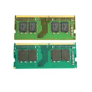
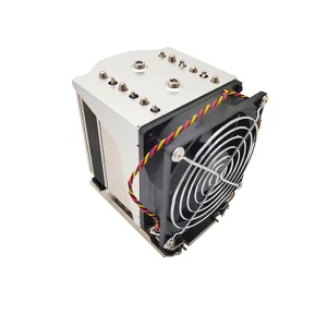
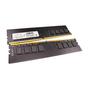
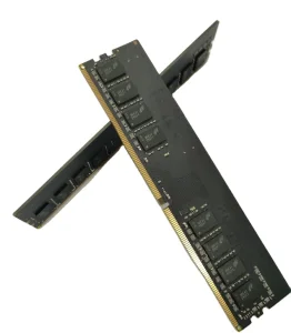
We combine high-density SMT layout capabilities with robust heat sinks. This design satisfies high-speed DDR4/DDR5 signaling needs while routing intense power levels directly through inner thick copper cores.

Industrial Control Units

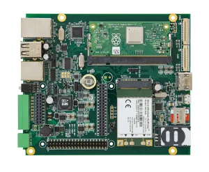
Our ODM solutions, including Raspberry Pi style control boards, integrate heavy copper to maintain physical rigidity and EMI shielding in noisy industrial environments subject to continuous thermal cycling.

Technology Roadmap & Engineering Futures

Mapping out next-generation manufacturing capabilities, material hybrids, and SMT developments.

1. Advanced Fabrication and Etching Challenges

Etching thick copper features requires specialized chemistry and process control. As copper thickness increases, lateral etching (undercutting) becomes more pronounced. Standard etching lines fail to preserve tight spacing. Our factory employs automated optical alignment and specialized acid etching lines to maintain minimum trace-and-space dimensions, even at 6 oz and higher weights.

Furthermore, filling the wide air gaps between thick copper tracks requires advanced resin prepregs. Standard resin systems can form voids during lamination, leading to electrical breakdown at high voltages. Corexis uses high-resin-content prepregs and customized vacuum press profiles to ensure void-free encapsulation of internal copper traces.

2. Material Integration: The Hybrid Stack Trend

Modern telecommunication and server power supply architectures cannot rely solely on standard FR4 substrates. To minimize costs while meeting speed and thermal demands, Corexis engineers develop hybrid stack-ups. In these designs, high-frequency materials (such as Rogers 4350B or Rogers 4003C) are co-laminated with heavy copper power plane layers on TG170/TG180 FR4 bases. This approach delivers optimal RF performance and high-current capability in a single board structure.

Localization, Compliance & Quality Inspection Workflows

Corexis applies strict verification protocols to maintain absolute reliability across all shipped batches.

To support global supply chains in highly regulated industries, our manufacturing quality control process features five primary check stages:
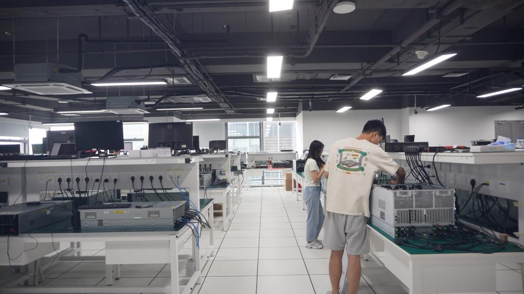
  1. Incoming Material Inspection (IQC): Every batch of copper foil, FR4 laminate, memory chip (DRAM), and chemical agent undergoes spectroscopy and thickness verification to confirm compliance with international guidelines.
  2. In-Process Quality Control (IPQC): Real-time laser profiling monitors copper trace thickness after etching, and Automated Optical Inspection (AOI) scans layer registration prior to final multi-layer lamination.
  3. Final Quality Control (FQC): 100% electrical testing (flying probe or grid fixtures) checks for micro-shorts and open circuits, ensuring electrical continuity across high-current channels.
  4. Outgoing Quality Assurance (OQA): Visual and dimensional inspection checks surface finishes, solder mask thickness, and overall board edge tolerances before packaging.
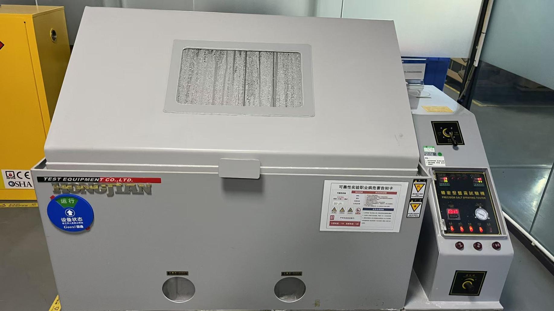
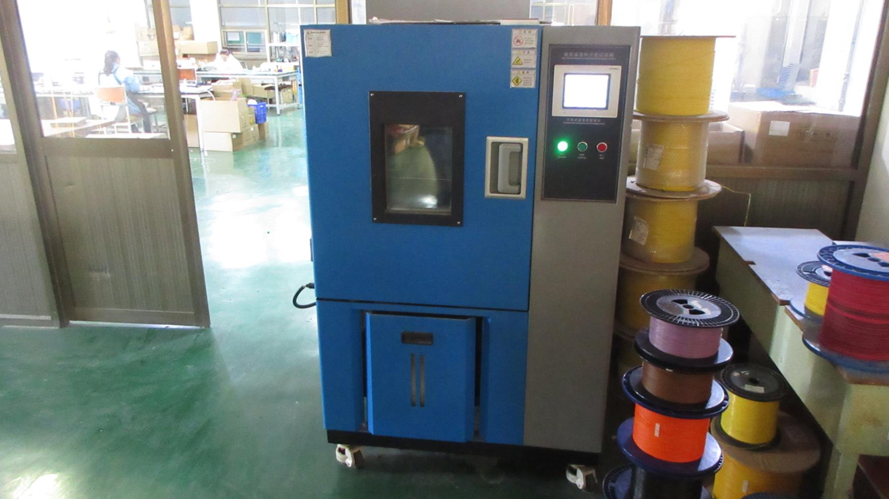
  5. Reliability & Compatibility Testing: Micro-sectioning analysis confirms plating thickness inside plated through-holes (PTH), while thermal shock tests check for resistance to delamination under reflow temperatures.

Factory Facility & Manufacturing Process

Technical Q&A: Sourcing & Engineering Guidance

Answers to common industry queries regarding thick copper manufacturing and quality assurance.

What constitutes a "Thick Copper PCB" or "Heavy Copper PCB"?
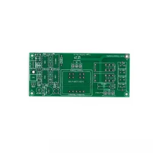
Generally, any printed circuit board featuring copper weights of 3 oz/ft² (105µm) to over 20 oz/ft² (700µm) on either internal or external layers is considered a heavy copper PCB. Extreme copper boards can exceed 20 oz/ft², using specialized chemical etching and plating techniques to handle high current loads and assist with heat dissipation.
How does thick copper improve thermal performance?
Thick copper planes act as effective heat spreaders, conducting thermal energy away from high-power components (like power transistors or CPUs) toward thermal vias or integrated heat sinks. This design minimizes localized hot spots and improves reliability without requiring loud external cooling systems.
Can you combine high-frequency signals with thick copper power planes?
Yes. Through hybrid multi-layer stack-ups, we can laminate high-speed substrates (e.g., Rogers 4000 series or high-TG FR4) on top of heavy copper power cores. This allows designers to place high-speed control logic and high-current power networks on a single PCB, saving space and improving signal integrity.
What are the primary fabrication challenges with heavy copper?
The main challenges include controlling trace undercut during etching, achieving uniform solder mask coverage on trace edges, and preventing voiding in the dielectric spacing. Corexis utilizes advanced high-pressure etching lines and high-flow resin prepregs to manage these issues.
Does Corexis offer complete ODM motherboard SMT assembly for heavy boards?
Yes, we provide full ODM and OEM services, including custom PCB design, SMT component assembly, and hardware testing. Our SMT production lines are optimized to handle heavy-mass PCBs, adjusting reflow profiles to prevent cold solder joints and component shifting.