Engineered to support fine-pitch solder deposition, high speed components, and advanced PCB layouts in Rio Grande, Buenos Aires, and beyond.
A Comprehensive Whitepaper on Micro-Aperture Engineering, Material Deposition, and Supply Chain Resiliency in South America's Emerging High-Tech Corridors.
Argentina's electronics manufacturing ecosystem is uniquely structured, with its primary core established in the Special Economic Area of Tierra del Fuego (Ushuaia and Río Grande), operating under Law 19,640. This region, alongside industrial parks in Buenos Aires, Rosario, and Córdoba, focuses heavily on domestic assembly of consumer electronics, automotive ECUs, home appliances, and telecommunications equipment.
For Argentinian OEMs and Contract Manufacturers (EMS), securing a reliable, high-yield pipeline of SMT (Surface Mount Technology) components and assembly tooling is a critical parameter. Modern high-density PCBs require ultra-precise SMT laser stencils to ensure defect-free solder paste printing. Without precise stencil geometry, assemblies suffer from bridging, solder balling, or starved joints, leading to high rework rates that damage productivity under tight import and economic environments.
As components shrink from 0603 to 0201 and down to 01005 passives, combined with fine-pitch micro-BGA packages, SMT stencil design has moved from mechanical chemical etching to advanced laser cutting and micro-polishing. The technological roadmap of laser stencils involves three key innovations:
An overview of physical parameters and engineering tolerances required for modern fine-pitch surface mount assembly.
To achieve high-efficiency solder paste transfer for components like high-speed DDR4/DDR5 memories and dense Rockchip system-on-modules, engineering guidelines state that the Area Ratio of the aperture must be kept strictly above 0.66. Below this threshold, transfer efficiency drops dramatically unless nanocoatings are implemented.
| Stencil Parameter / Feature | Standard Fine-Pitch | Advanced Ultra-Fine-Pitch | High-Precision Nano-Coated |
|---|---|---|---|
| Base Foil Material | SUS304 Full Hard Stainless Steel | Fine Grain (FG) Stainless Steel | FG Stainless Steel with Hydrophobic Coating |
| Foil Thickness Range | 100µm - 150µm (±3µm) | 80µm - 120µm (±2µm) | 50µm - 100µm (±1.5µm) |
| Min. Aperture Width | 120 µm | 80 µm | 60 µm |
| Aperture Corner Radius | R20 µm to R30 µm | R15 µm to R20 µm | R10 µm |
| Wall Taper Angle | 1.5° - 2.5° (Inverted trapezoid) | 1.0° - 1.5° | < 1.0° (Optimal Release) |
| Target Components | QFP 0.5mm, 0402 Passives | BGA 0.4mm, 0201 Passives | MicroBGA 0.3mm, 01005, WLCSP |
By leveraging high-speed fiber-laser machines running under thermal stabilization, modern manufacturers cut over 15,000 apertures per hour with positional accuracies of ±5 µm, ensuring that the stencils align perfectly with the multi-layer boards destined for Argentine electronic assemblers.
Scaling Global Exports with Smart SMT Production and Robust Material Engineering
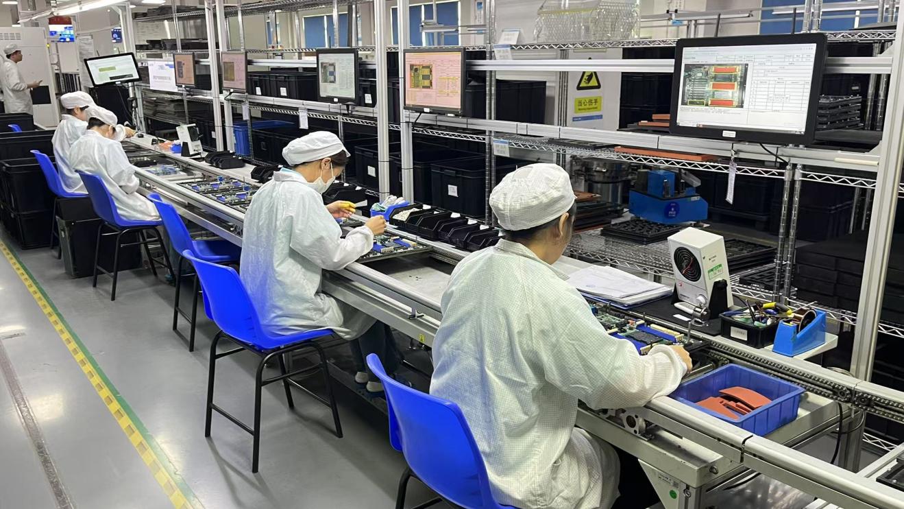
Founded in 2016, Corexis has spent a decade refining the boundaries of high-speed SMT assembly, memory chip packaging, and hardware optimization. Our state-of-the-art facility integrates advanced SMT lines with high-speed AOI, 3D SPI (Solder Paste Inspection), and dedicated laser cutting units for internal and custom stencil manufacturing.
As a vertically integrated manufacturer, we understand that stencil accuracy directly dictates product yield. Our 56 quality control staff run comprehensive checks using automatic optical scanners to inspect every single laser aperture against original Gerber files before clean-room packaging.
Securing tooling for assembly lines in Tierra del Fuego or industrial hubs in Buenos Aires presents complex logistical challenges. Heavy customs requirements (such as SIMI/SIRA processing) and maritime shipping times demand an agile supplier.
Corexis partners with premium global logistics providers, packaging stencils in vacuum-sealed moisture-barrier bags inside ruggedized wooden crates. This ensures they arrive at their South American destination without tension degradation, surface oxidation, or structural warping. Our typical manufacturing lead time for standard framed or frameless laser stencils is under 24 hours from Gerber approval, backed by expedited air freight options to Buenos Aires.
Targeted Engineering Solutions Specially Curated for Argentine Local Assemblies
For Tier-1 automotive suppliers in Buenos Aires and Córdoba, component placement must adhere to rigid zero-defect automotive standards (AEC-Q100). We design stepped stencils that allow large, high-power connector pads to receive thick solder paste layers while simultaneously applying precise, thin deposits for fine-pitch sensor microcontrollers on the same board.
Argentine assembly centers in Ushuaia produce millions of TVs, air conditioners, and cellular systems. Our high-durability nano-coated stencils enable continuous SMT print runs with up to 70% fewer wipe cycles. This dramatically boosts machine utilization rates and decreases isopropyl alcohol consumption in local manufacturing facilities.
For heavy industrial and solar inverter systems assembled locally in Argentina, thick-copper PCBs are standard. Thick copper creates surface topography that poses major challenges for standard flat stencils. Our custom stepped-stencils bridge these uneven copper layers seamlessly, ensuring reliable solder application across varying component dimensions.
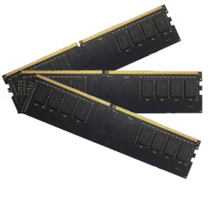
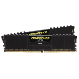
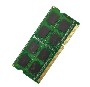
High-reliability modules designed to function seamlessly alongside high-precision PCB assembly tooling.
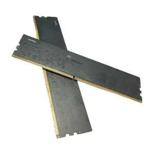
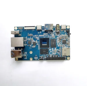
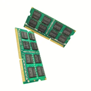
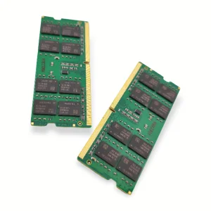
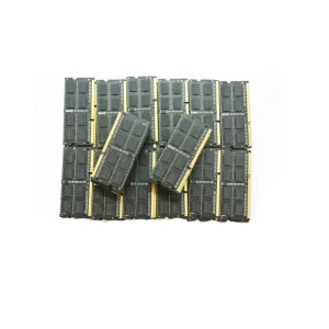
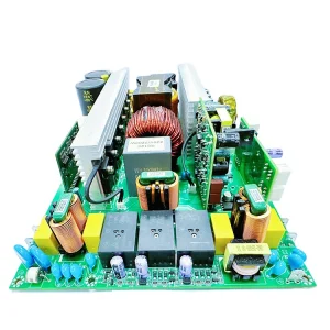
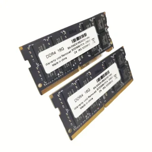
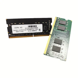
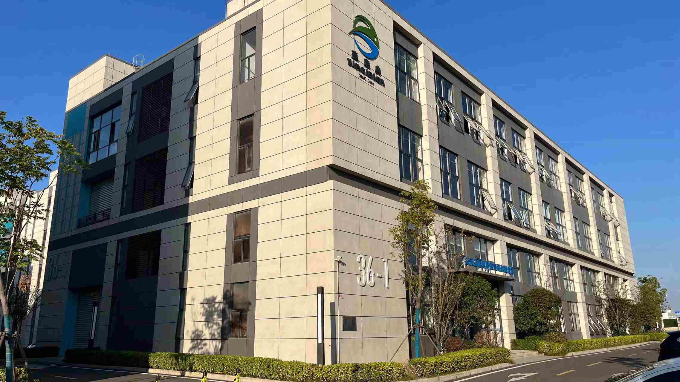
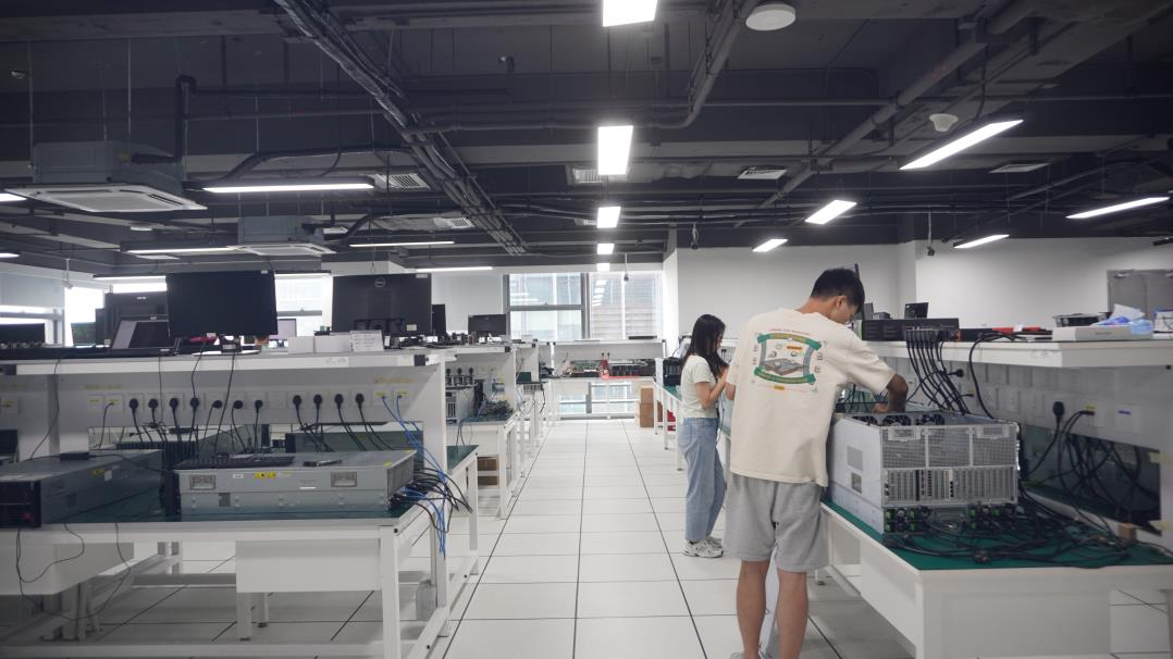
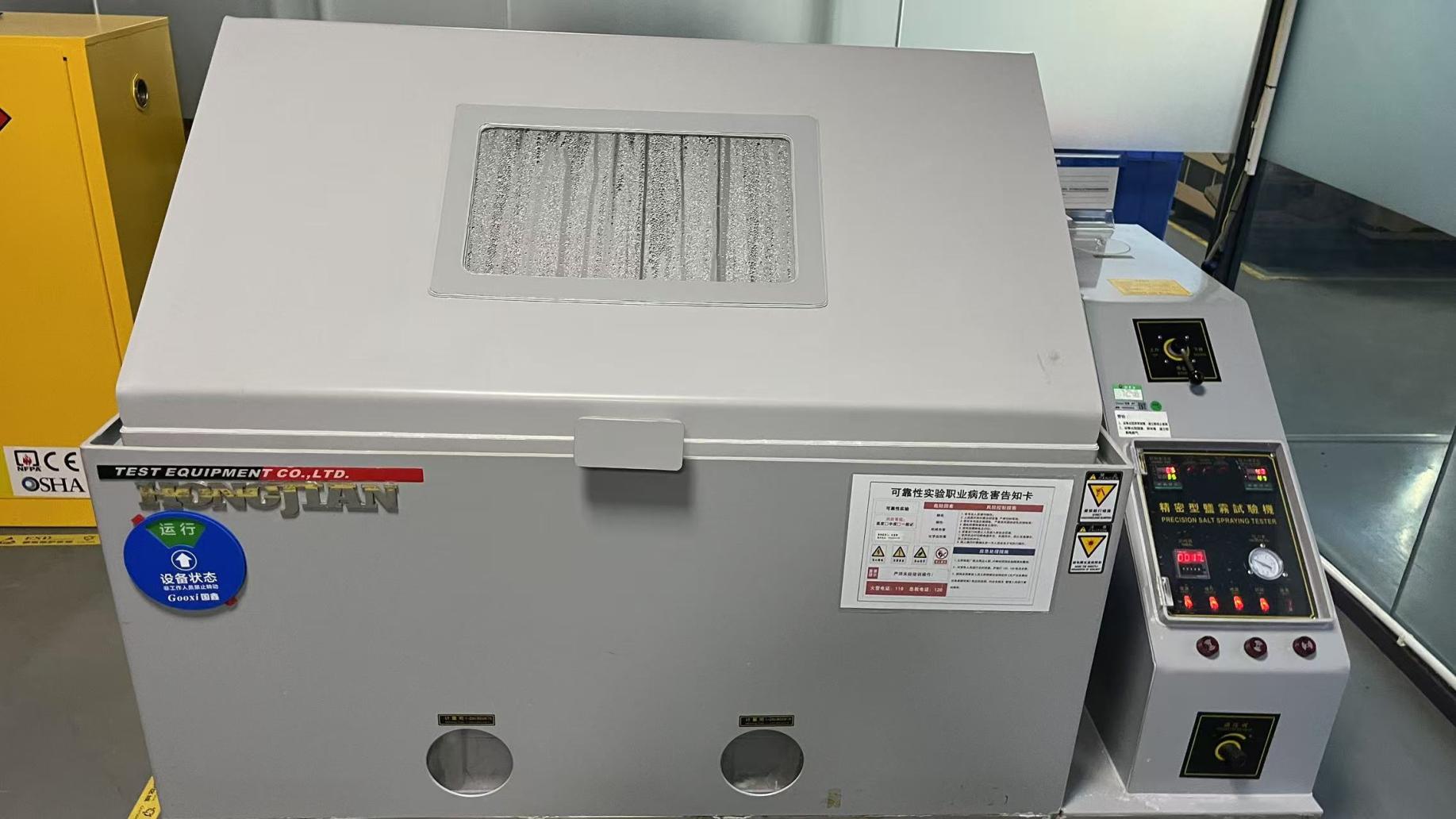
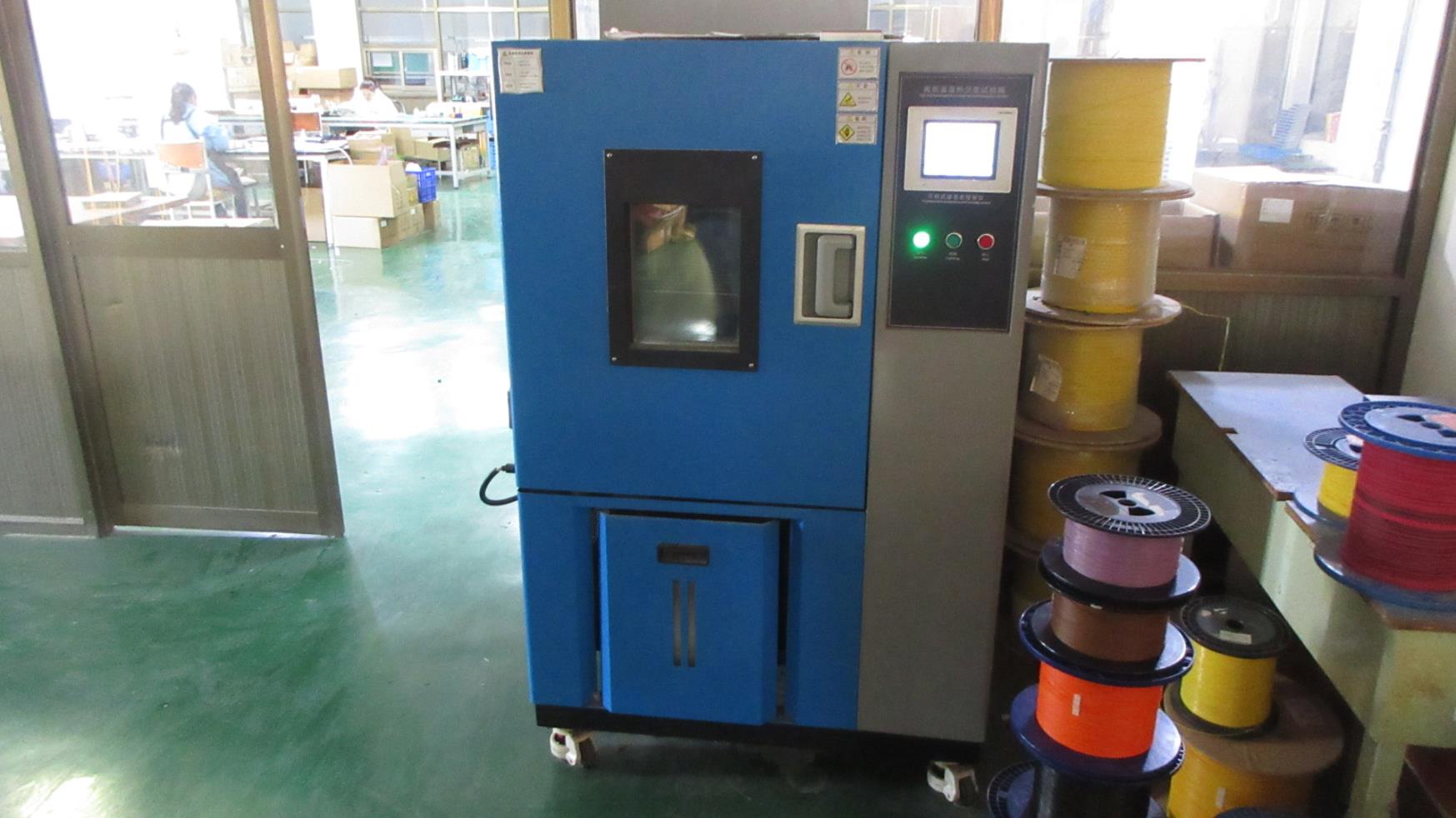
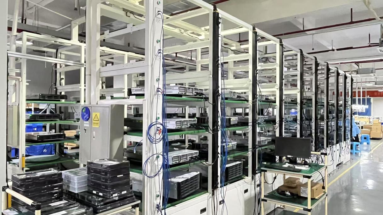
Explore our state-of-the-art 21,800 m² facility utilizing fully automated SMT equipment, laser manufacturing, and inspection environments.

Clear, analytical answers regarding laser stencils import, design considerations, and global supply workflows for Argentina.
Get a detailed engineering review of your SMT Gerber designs and premium memory component requirements from Corexis.
Send Inquiry Now Corexis Memory