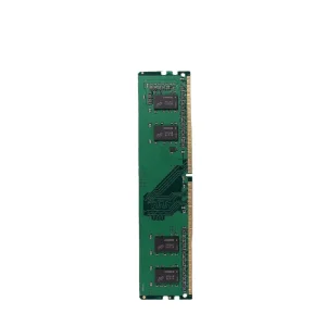
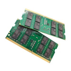
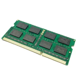
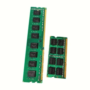
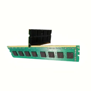
Browse our highly reliable DDR4 notebook/desktop RAM modules, manufactured using cutting-edge SMT processes and stringent component matching.
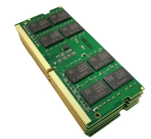
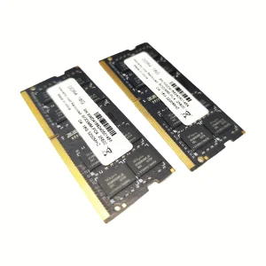
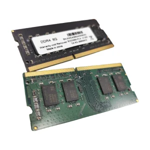
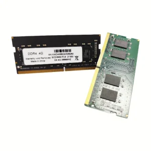
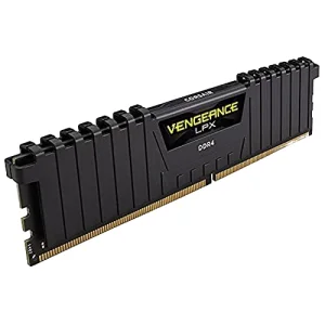
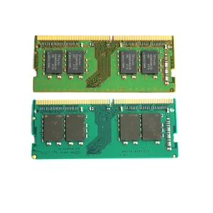
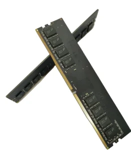
A comprehensive analysis of high-reliability Printed Circuit Board Assembly (PCBA), semiconductor integration, and hardware localization trends.
In the modern hardware sector, the complexity of Printed Circuit Board Assembly (PCBA) has risen exponentially. What once was a standard mounting process has evolved into an intricate micro-electronics integration practice. As device footprints shrink and computing demands increase, leading SMT manufacturers in China have expanded beyond assembly roles to serve as comprehensive development, engineering, and supply-chain partners.
The contemporary electronics ecosystem relies on high-speed data processing, advanced power management, and thermal stability. Devices ranging from aerospace circuitry to consumer-grade computing demand high component density, complex layer stacks, and high mechanical durability. To navigate these requirements, engineering teams require deep transparency regarding substrate materials, thermal management techniques, and component sourcing standards.
China's PCBA ecosystem stands at the center of this technological transition. Combining SMT technology with integrated semiconductor packaging enables local manufacturers to address challenges across automotive, industrial IoT, medical devices, high-speed computing, and telecommunications. This deep-dive whitepaper explores the critical engineering paths, quality benchmarks, and industry solutions defining high-tier PCBA production today.
Established in 2016, Corexis Memory Technology Co., Ltd. is a specialized DDR5 memory manufacturer and electronics assembly provider. We focus on high-performance DRAM solutions, complex SMT assembly, and custom packaging systems for global OEM, ODM, and enterprise customers.
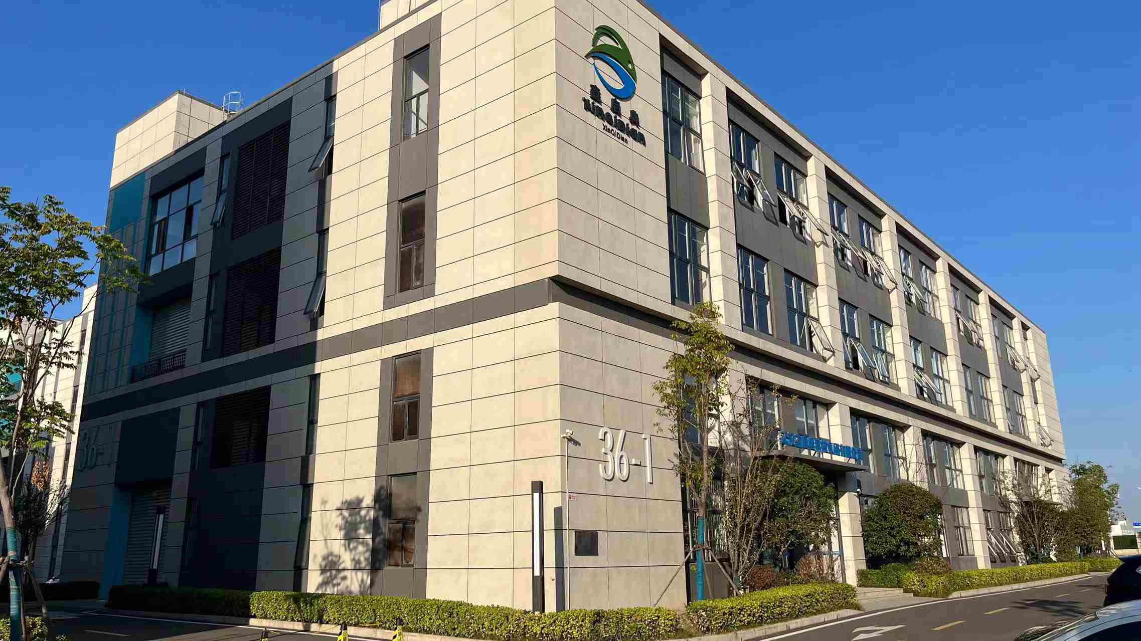
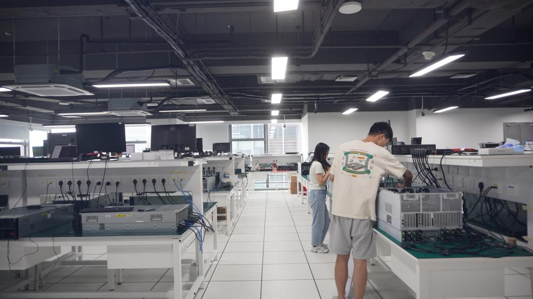
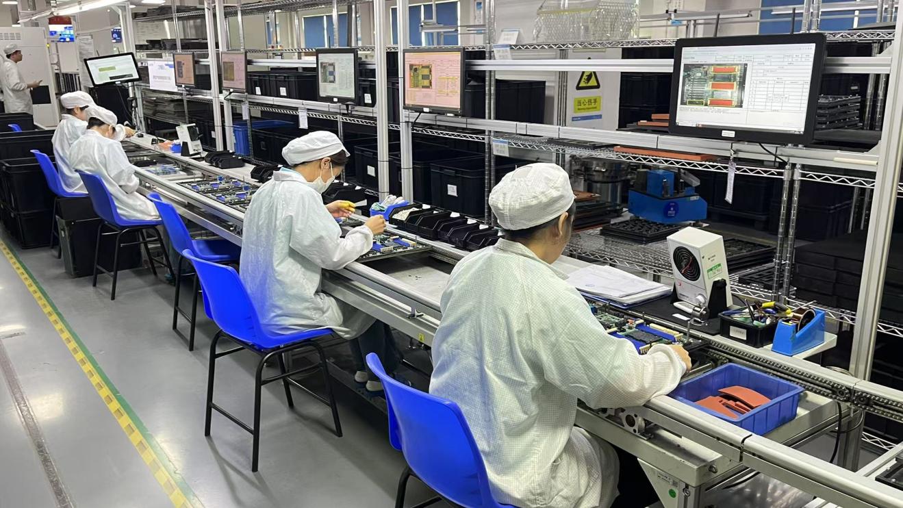
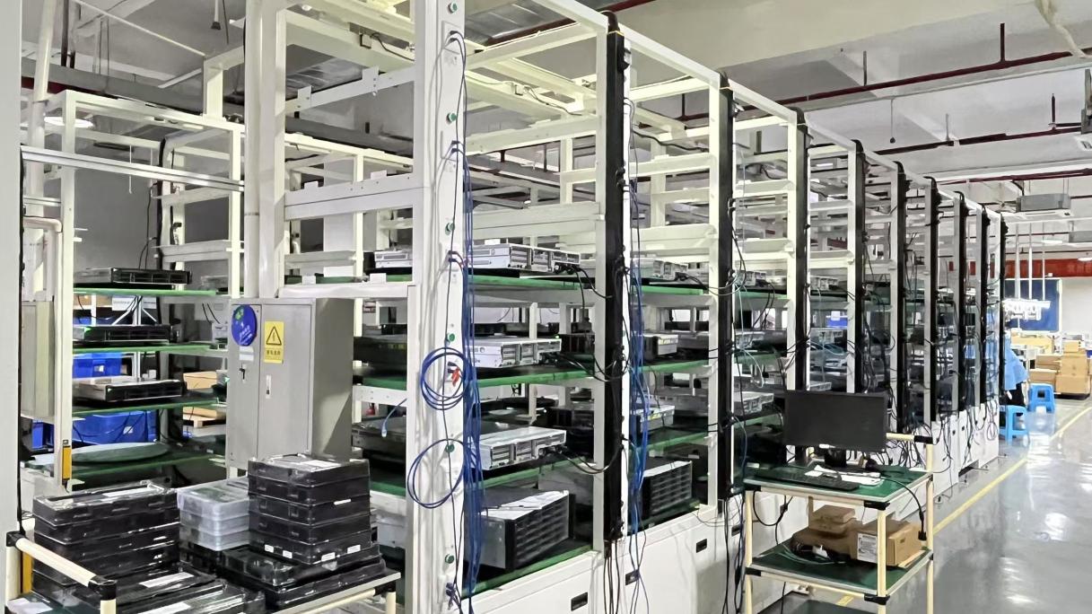
Operating a modern 21,800 m² manufacturing facility, our processes integrate design, SMT placement, advanced cleanroom testing, and quality control under one roof. Our engineering team designs and manufactures memory modules and complex board assemblies that meet rigorous international industry standards.
By pairing component-level expertise (such as high-speed DRAM packaging) with system-level PCBA production, we help customers bridge the gap between high-frequency semiconductor layout and production-ready hardware.
| Founded | 2016 |
| Factory Footprint | 21,800 m² |
| Annual Export Revenue | USD 26,800,000 |
| Industry Experience | 10 Years |
| R&D Engineering Team | 128 Specialists |
| Quality Control Staff | 56 QC Inspectors |
Ensuring stable supply chains and product longevity through data-driven manufacturing processes.
How modern PCB assembly meets the performance, thermal, and regulatory needs of key industrial sectors.
High-speed server environments require stable memory interfaces and low parasitic inductance. By aligning DDR4/DDR5 manufacturing with strict signal-integrity routing, we support robust system integration for data centers, embedded IPCs, and cloud storage systems.
Precision electronics, such as industrial metal detectors, rely on micro-volt signal changes. Preventing signal degradation requires low-loss substrate material selection, isolated ground planes, and precise analog layout structures to minimize cross-talk.
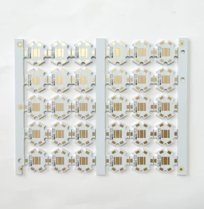
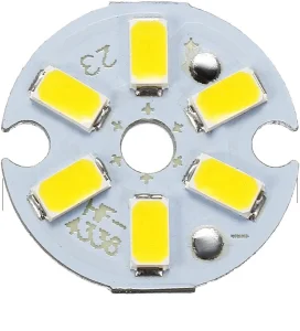
High-power LED systems (such as T6, 5050, and 3535 lamp beads) produce significant thermal output. Metal core PCBs (MCPCBs), particularly aluminum substrates, are used to transfer heat away from critical component junctions, extending device lifetimes.
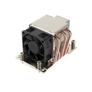
High-density processors (such as the AMD SP6 socket) need dedicated thermal management. Combining active thermal blocks with 350W-rated coolers ensures that high-speed hardware maintains optimal operating temperatures during sustained workloads.
Automotive assemblies demand resistance to thermal cycles, moisture, and vibration. Meeting these requirements involves using specialized underfills, select conformal coatings, and robust lead-free solder alloys to secure critical joints.
Rapid consumer development relies on short lead times and accurate prototyping. Our flexible manufacturing pathways support low-volume prototype builds, validating designs prior to transitioning to high-speed mass production runs.
Ensuring electrical, mechanical, and thermal stability in high-density multi-layer printed circuit board assemblies.
In high-frequency applications, trace layout acts as a transmission line. We use modern modeling tools to optimize characteristic impedance for differential pairs, DDR data buses, and clock signals. Controlling dielectric thickness (using FR4, Rogers, or PTFE) and copper thickness ensures minimal signal attenuation and distortion.
Modern ball grid arrays (BGAs) and chip-scale packages (CSPs) feature pitches below 0.4mm. Our pick-and-place lines use vision alignment systems to place components down to 01005 passives. Maintaining accurate solder paste deposits requires using laser-cut stencils with nano-coatings and automatic 3D Solder Paste Inspection (SPI).
Reflow profiles must balance wetting and component heat limits. Multi-zone convection ovens, running under nitrogen environments, help reduce solder joint oxidation. For bottom-terminated components, we control outgassing to keep solder voiding rates well below IPC-A-610 limits, avoiding potential hotspots.
| Process Capability | Standard Requirement | Corexis Advanced Limits |
|---|---|---|
| Min Component Size | 0402 Imperial | 01005 (0402 Metric) |
| BGA Ball Pitch | ≥ 0.5 mm | ≥ 0.35 mm (with 3D X-Ray Inspection) |
| Max PCB Dimensions | 400 x 400 mm | 610 x 508 mm |
| PCB Layer Count | 1 - 12 Layers | Up to 32 Layers (HDI, Blind/Buried Vias) |
| Quality Classification | IPC Class 2 | IPC Class 3 (High-Reliability / Industrial) |
Component sourcing integrity is critical to avoiding counterfeit parts. We partner with verified global wafer foundries and component distributors. Every batch undergoes Incoming Quality Control (IQC) checking, and DRAM components are matched for speed, latency, and thermal performance.
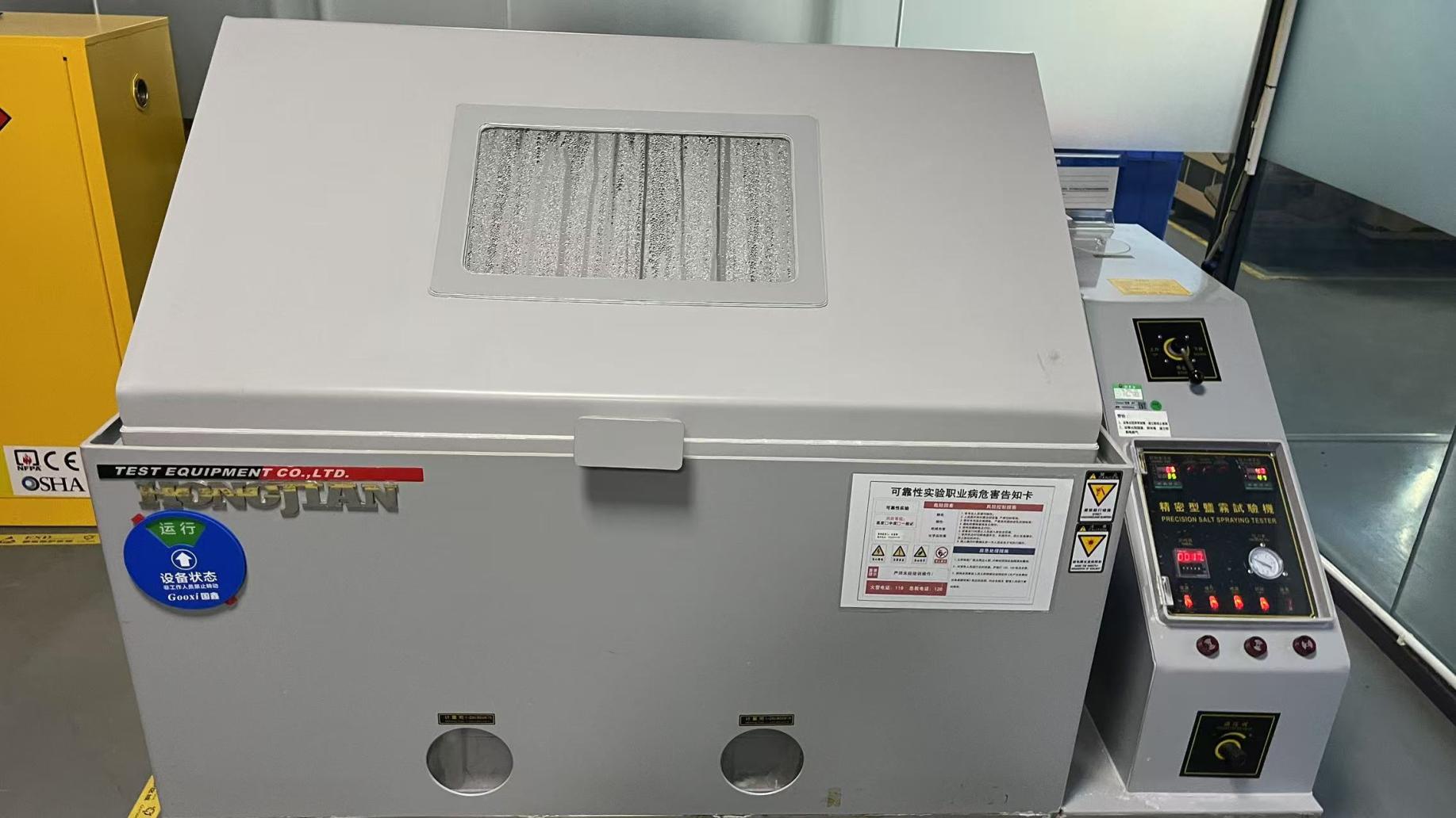
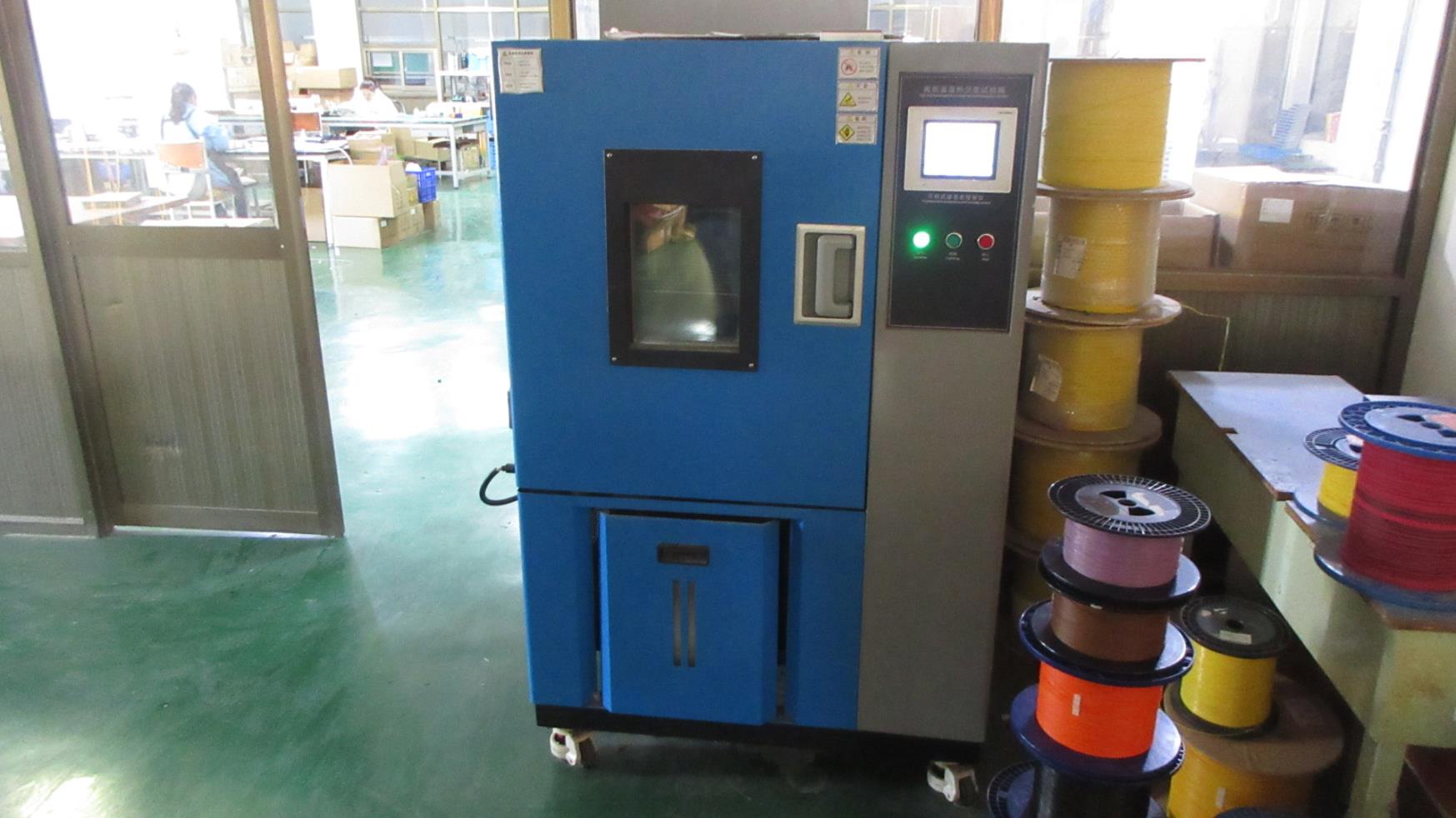
Our quality control process is managed by 56 dedicated specialists across five stages: IQC (Incoming), IPQC (In-process), FQC (Final), OQA (Outgoing), and regular environmental stress screening (ESS).
Advanced diagnostic tools, including 3D X-ray (AXI), Automated Optical Inspection (AOI), and in-circuit testers (ICT), help verify each solder joint and internal trace before packaging.
Ensuring compliance with environmental and logistical regulations across global jurisdictions.
Navigating global electronics logistics requires compliance with various regional regulations. Our products and processes are aligned with global trade frameworks to support smooth shipping and customs integration:
Additionally, our logistics and engineering teams assist global OEM/ODM partners with customs clearance, import documentation, and localized technical support across North America, Europe, and the Asia-Pacific region.

A preview of coming changes in component integration, board structures, and manufacturing processes.
As computing requirements continue to scale, hardware engineering is shifting toward more integrated chip structures and higher frequencies. These trends shape our technology roadmap:
DDR5 and future DDR6 architectures move power management directly onto the module via PMICs (Power Management Integrated Circuits). This design improves power efficiency but increases thermal density on the PCB. Designing these modules requires careful layer stackups and power plane layout to avoid local hotspots.
To reduce trace lengths and parasitic capacitance, manufacturers are increasingly embedding passive components directly within substrate layers. This approach frees up surface space for active ICs and improves high-frequency signal characteristics.
We are incorporating real-time SMT line feedback loops, where SPI systems automatically communicate coordinate corrections to printing presses. This closed-loop configuration reduces placement defect rates and maintains yields during high-volume production runs.
Answers to technical and logistical questions commonly raised by procurement and engineering teams.
Explore our manufacturing options, including aluminum boards, active cooling assemblies, and specialized memory modules.
 Corexis Memory